


6-6
MPC8240 Integrated Processor User’s Manual
SDRAM Interface Operation
6.2 SDRAM Interface Operation
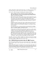
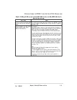
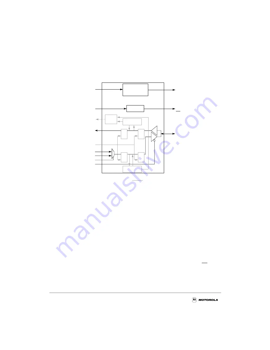
Figure 6-2 shows an internal block diagram of the SDRAM interface of the MPC8240.
Figure 6-2. SDRAM Memory Interface Block Diagram
The MPC8240 provides control functions and signals for JEDEC-compliant SDRAM. The
MPC8240 supplies the SDRAM_CLK[0:3] to be distributed to the SDRAM. These clocks
are the same frequency and in phase with the memory bus clock.
The SDRAM memory bus can be configured to be 64 bits (72 bits with parity) requiring a
four-beat SDRAM data burst, or configured to be 32 bits (36 bits with parity) requiring an
eight-beat SDRAM data burst.
Twelve row/column multiplexed address signals (SDMA[11:0]) and two bank select
signals (SDBA[1:0]) provide SDRAM addressing for up to 16 M. The data width of the
device determines its density and the physical bank size. Eight chip select signals (CS[0:7])
support up to eight banks of memory. Eight SDRAM data in/out mask signals (DQM[0:7])
provide byte selection for 32- and 64-bit accesses. Thus, an 8-bit SDRAM device has a
DQM signal and eight data signals (DQ[0:7]). A 16-bit SDRAM device has two DQM
signals associated to specific halves of the sixteen data signals (DQ[0:7] and DQ[8:15]).
SDRAM
SDRAM
Address
Row
Col
Address
(Processor or PCI)
SDRAM Memory Control
Data from Peripheral Logic
Data from Processor Core
Data from SDRAM
SDRAM write source select
SDRAM write output enable
Central Control Unit
SDRAM Memory Interface
SDRAM Memory Array
Data Pins
MDH[0:31]
MDL[0:31]
Control
MUX
SDMA[12:0]
CS[0:7]
DQM[0:7]
QD
QD
QD
QD
Internal Bus Clock
64-bit
In-Line ECC
64-bit
In-Line ECC
Error
Signals
Error Signals to
Peripheral Logic
Note:
Selectable Buffering
PAR[0:7]
SDBA[1:0]
1. Flow-through (default mode)
2. Registered
Error Checking
1. Registered w/64-bit In-Line ECC
2. Parity
Содержание MPC8240
Страница 1: ...MPC8240UM D Rev 1 1 2001 MPC8240 Integrated Processor User s Manual ...
Страница 38: ...xviii MPC8240 Integrated Processor User s Manual TABLES Table Number Title Page Number ...
Страница 48: ...xlviii MPC8240 Integrated Processor User s Manual Acronyms and Abbreviations ...
Страница 312: ...6 94 MPC8240 Integrated Processor User s Manual ROM Flash Interface Operation ...
Страница 348: ...7 36 MPC8240 Integrated Processor User s Manual PCI Host and Agent Modes ...
Страница 372: ...8 24 MPC8240 Integrated Processor User s Manual DMA Register Descriptions ...
Страница 394: ...9 22 MPC8240 Integrated Processor User s Manual I2O Interface ...
Страница 412: ...10 18 MPC8240 Integrated Processor User s Manual Programming Guidelines ...
Страница 454: ...12 14 MPC8240 Integrated Processor User s Manual Internal Arbitration ...
Страница 466: ...13 12 MPC8240 Integrated Processor User s Manual Exception Latencies ...
Страница 516: ...16 14 Watchpoint Trigger Applications ...
Страница 538: ...B 16 MPC8240 Integrated Processor User s Manual Setting the Endian Mode of Operation ...
Страница 546: ...C 8 MPC8240 Integrated Processor User s Manual ...
Страница 640: ...INDEX Index 16 MPC8240 Integrated Processor User s Manual ...


