background image

MOTOROLA

MC68838 USER’S MANUAL

2-7

This logic block is connected to the receive data path to be able to load a bid time
register from claim frames that are being received. ln addition, it receives signals to
enable/disable the TVX timer and to reset the TVX timer from the receiver FSM. Its only
outputs (other than to the NPI) are TRT expired, TVX expired, THT expired, and
LATE_CT equals zero interrupts.

2.3.7 Transmit Data Latch (and Repeat Function)

This logic block contains the repeat function and multiplexes the repeat path with
FRAME_DATA from the send frame logic block. The repeat function reads symbol pairs
from the receive data path and repeats them to the ELM. Usually this logic transmits the
symbol pair just received, but when receiving the FS indicators, the logic may need to
modify the received R and S symbols according to the values in the frame status logic
and the values in the register associated with repeating additional FS symbols. Also, this
logic selectively replaces the last symbol pair with an IDLE symbol pair when a frame is
detected as a fragment.

2.4 TEST AND CLOCK LOGIC

The MAC supports complete boundary scan testing and random access reading of
almost all of the internal chip state through the NPI. Boundary scanning means that
every signal on this chip (other than the 

MATCH signal, the test signals, and clocks) has

an associated scan latch that enables the testing interface to serially shift in an arbitrary
bit pattern to be used for the corresponding input or output signal and to shift out the
values of these signals while holding the clock. The MAC also has a built-in self-test
capability.

ARCHIVE INFORMA

TION

ARCHIVE INFORMA

TION

Содержание MC68838

Страница 1: ... application in which the failure of the Motorola product could create a situation where personal injury or death may occur Should Buyer purchase or use Motorola products for any such unintended or unauthorized application Buyer shall indemnify and hold Motorola and its officers employees subsidiaries affiliates and distributors harmless against all claims costs damages and expenses and reasonable...

Страница 2: ...en referring to items in the manual please reference by the page number paragraph number figure number table number and line number if needed Reference the line number from the top of the page When we receive a FAX between the hours of 7 30 AM and 5 00 PM EST Monday through Friday we will respond within two hours If the FAX is received after 5 00 PM or on the weekend we will respond within two hou...

Страница 3: ...4 2 3 Transmit Data Path 2 4 2 3 1 Transmit Data Host lnterface 2 5 2 3 2 Send Frame Logic 2 5 2 3 3 Capture Token Logic 2 5 2 3 4 Transmit CRC Generator 2 6 2 3 5 Transmit Finite State Machine 2 6 2 3 6 Timers 2 6 2 3 7 Transmit Data Latch and Repeat Function 2 7 2 4 Test and Clock Logic 2 7 Section 3 Register Description 3 1 Register Types 3 3 3 1 1 Read Write Registers 3 3 3 1 2 Read Control Wr...

Страница 4: ...MLA_C 3 26 3 5 3 Target Request Time Register T_REQ 3 26 3 5 4 TVX TRT Initial Timer Parameter Register TVX_VALUE T_MAX 3 26 3 6 Protocol Timing Registers 3 27 3 6 1 TVX Timer Register TVX_TIMER 3 27 3 6 2 TRT Timer Register TRT_TIMER_A TRT_TIMER_B 3 27 3 6 3 THT Timer Sent Count Registers THT_TIMER_A THT_TIMER_B SENT_COUNT 3 28 3 6 4 TRT Time Remaining Register T_NEG_A T_NEG_B 3 29 3 6 5 Informat...

Страница 5: ...Data Path Control 8 1 8 2 MAC Packet Transmission 8 3 8 3 Packet Request Header 8 4 Section 9 CAM Interface Operation 9 1 CAM Interface Operation 9 1 9 1 1 Normal Nonextended Match Mode 9 1 9 1 2 Extended Match Mode 9 2 9 2 Extensions to A and C Bit Handling 9 4 Section 10 Test Operation 10 1 Built In Self Test Operation 10 1 10 2 Scan Path Operation 10 2 Section 11 Electrical Characteristics 11 1...

Страница 6: ...ELM Timing 11 5 11 8 CAM Interface Timing 11 6 Section 12 Ordering Information and Mechanical Data 12 1 Ordering Information 12 1 12 2 Pin Assignments 12 2 12 2 1 120 Lead Ceramic Pin Grid Array w Ceramic Lid KB 12 2 12 2 2 120 Lead Plastic Quad Gull Wing FC 12 3 12 3 Package Dimensions 12 4 ARCHIVE INFORMATION ARCHIVE INFORMATION ...

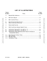
Страница 7: ... Bus Write Cycles 5 3 7 1 Receive Data Flowchart 7 4 8 1 TXRDY and Packet Request Header Timing 8 2 9 1 CAM Interface Signals EXT_DA_MATCH 0 9 2 9 2 CAM Interface Signals EXT_DA_MATCH 1 9 3 9 3 CAM Interface Timing Receiving Token Frame for Normal and Extended Match Mode 9 3 11 1 Node Processor Interface Timing 11 3 11 2 MAC FSI Timing 11 4 11 3 MAC ELM Timing 11 5 11 4 CAM Interface Timing 11 6 A...

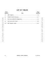
Страница 8: ...IST OF TABLES Table Page Number Title Number 3 1 MAC Registers 3 2 6 1 RCDATx TXDATx Encoding 6 1 7 1 RCCTLx and RPATHx Relationship 7 3 9 1 MAC A and C Bit Control 9 4 10 1 BIST Register Values 10 2 ARCHIVE INFORMATION ARCHIVE INFORMATION ...

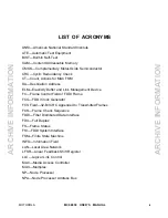
Страница 9: ... and Link Management Device FC Frame Control Field of FDDI Frame FCG FDDI Clock Generator FCS Field 32 Bit CRC Appended to Transmitted Frames FCS Frame Check Sequence FDDI Fiber Distributed Data Interface FDX Full Duplex FS Frame Status FSI FDDI System Interface FSM Finite State Machine INFO Information Field LAN Local Area Network LFSR Linear Feedback Shift Register LLC Logical Link Control MAC M...

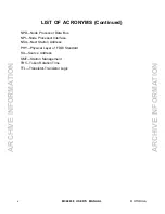
Страница 10: ...ued NPD Node Processor Data Bus NPI Node Processor Interface NSA Next Station Address PHY Physical Layer of FDDI Standard SA Source Address SMT Station Management TRT Token Rotation Time TTL Transistor Transistor Logic ARCHIVE INFORMATION ARCHIVE INFORMATION ...

Страница 11: ...AM INTERFACE USER SYSTEM PAL PIN AMPLIFIER DRIVER LED FROM FIBER OPTIC CABLE TO FIBER OPTIC CABLE OPTIONAL EXTERNAL CAM Figure 1 1 Motorola FDDI Architecture The ANSI standard specifies the data link MAC layer the physical and physical media dependent entities and the station management and submanagement physical connection management The MAC protocol the lower sublayer of the data link layer prov...

Страница 12: ...neously Generate and Check CRC Supports 16 Bit or 48 Bit Individual Station Addresses On Chip Contains an Interface to a CAM for Individual and Multicast Address Recognition Supports Several Bridging Facilities Can Reverse Bit Ordering on DA and SA Contains Count and Void Frame Bridge Stripping Algorithm On Chip Allows Generating Frame CRC on per Frame Basis Supports A and C Bit Handling for Trans...

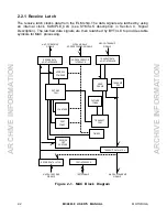
Страница 13: ... to the external RCDATx bus data bus from the ELM chip through a pipeline latch in the receive latch logic and to the RPATHx data bus to the FSI chip Only the receive data latch containing the current received symbol pair drives this internal data bus Usually several different logic blocks are concurrently reading and processing this symbol pair These logic blocks perform the following functions D...

Страница 14: ...bols for MAC processing RECEIVE DATA LATCH TRANSMIT DATA LATCH TIMERS TRANSMIT FSM RECEIVE CRC CHECKER SENT COUNT COUNTERS CAPTURE TOKEN TRANSMIT CRC RECEIVE FSM RECEIVE DATA HOST INTERFACE TRANSMIT DATA HOST INTERFACE NODE PROCESSOR INTERFACE TEST INTERFACE SEND FRAME ADDRESS COMPARE MAC PHY RECEIVE SIGNALS TEST SIGNALS MAC PHY TRANSMIT SIGNALS MAC FSI RECEIVE SIGNALS CLOCK SIGNALS NODE PROCESSOR...

Страница 15: ...number of error frames i e frames containing a bad CRC or an invalid data length that were detected by this station but by no previous station since the last time this counter was read and reset or the chip was reset Lost_Ct is a 6 bit unsigned count of the number of frame format errors that have occurred since the last time this counter was read and reset or the chip was reset Token_Ct is a 16 bi...

Страница 16: ...ceive FSM controls this logic and the results of the comparison are passed to the receive FSM 2 2 7 Receive Host Interface The FSI receive logic controls the RPATHx bus and RCCTLx bus that pass received frames to the FSI lt strips off the delimiters before passing the frame to the FSI lt handles all the extra control and handshake lines required for the RPATHx bus The receive FSM controls this log...

Страница 17: ...his logic does not communicate with the FSI receive logic 2 3 2 Send Frame Logic The send frame block is responsible for the actual transmission of a frame including the sequencing and sending of i e multiplexing of the preamble the appropriate delimiters e g JK TR RR etc the FC field for token claim beacon and void frames the DA and SA fields for claim beacon and void frames where they could be m...

Страница 18: ...INFO and TVX_VaIue and the LATE_CT The MAC standard specifies an additional register T_Opr which can contain redundant information and therefore is not implemented The TVX timer is used to ensure that a good frame i e correct CRC and valid data length or a nonrestricted token is seen by this station on every regular basis It can be used to detect events such as a babbling station an infinitely cir...

Страница 19: ...en receiving the FS indicators the logic may need to modify the received R and S symbols according to the values in the frame status logic and the values in the register associated with repeating additional FS symbols Also this logic selectively replaces the last symbol pair with an IDLE symbol pair when a frame is detected as a fragment 2 4 TEST AND CLOCK LOGIC The MAC supports complete boundary ...

Страница 20: ...2 8 MC68838 USER S MANUAL MOTOROLA ARCHIVE INFORMATION ARCHIVE INFORMATION ...

Страница 21: ... are accessible through the NPI are summarized in Table 3 1 When there is an A and B version of a register the A part holds the least significant bits and the B part holds the most significant bits The first hex digit of the address refers to NPA5 NPA4 and the second hex digit refers to NPA3 NPA0 ARCHIVE INFORMATION ARCHIVE INFORMATION ...

Страница 22: ...gister LOST_CT ERROR_CT 21 12 Read Only Clear Interrupt Event Register A INTR_EVENT_A 22 16 Read Only Clear Interrupt Event Register B INTR_EVENT_B 23 16 Read Only Clear Interrupt Event Register C INTR_EVENT_C 1D 3 Read Only Clear Receive Status Register RX_STATUS 24 16 Read Only Transmit Status Register TX_STATUS 25 16 Read Only TRT Time Remaining Register A T_NEG_A 26 16 Read Only TRT Time Remai...

Страница 23: ...automatically cleared when read by the NP If the MAC chip tries to modify a register that is being accessed by the NP the register is cleared and the MAC writes the new updated state The MAC chip can change these registers at any time even when the MAC FSMs are turned off These registers are all cleared by power up reset 3 1 4 Read Only Registers These registers can be read by the NP at any time b...

Страница 24: ...functions 3 2 1 Control Register A MAC_CNTRL_A Control register A controls the receiver portion of the MAC and a few joint receiver transmitter aspects The NP can read and write control register A at any time The MAC chip never modifies this register It is cleared on power up reset and unaffected by a MAC_Reset 2 14 13 12 11 10 9 8 MAC_ON SET_BIT_5 SET_BIT_4 REVERSE_ ADDR FLUSH_SA47 COPY_ALL COPY_...

Страница 25: ... The MAC chip will reverse the bit order of data octets passed to and from the FSI i e across RPATHx and TPATHx for all octets that make up the DA and SA fields of all frames to be sent or received from the FSI Therefore for DA and SA octets bit 7 x is passed to the FSI on RPATHx and bit 7 x is obtained from the FSI on TPATHx This feature is useful when implementing 802 3 and 802 4 protocol bridge...

Страница 26: ...n NSA frame The COPY_OWN mode of operation is not intended for normal operation but is reserved for special monitor stations and for ring loopback tests applicable to all stations 0 The MAC does not copy frames that it is currently sending nor frames that it believes it previously sent even if the MAC is requested to copy all frames with a certain FC or DA see the following register fields 1 The M...

Страница 27: ... of SMT frames i e SMT broadcast frames are always recognized and copied Unlike many register bits this bit still has an effect when COPY_ALL 11 or 10 Specifically this bit affects the 0D field of an END_DATA transfer for received broadcast frames 1 The MAC treats a MAC LLC implementor or reserved broadcast frame i e DA is all ones exactly as if it were another multicast frame of the same frame ty...

Страница 28: ...ime The MAC chip only modifies the RESET_FIELD bits The register is cleared on power up reset and is unaffected by a MAC_Reset 15 14 13 12 11 10 9 8 RING_PURGE FDX_MODE BRIDGE_STRIP TXPARITY_ON REPEAT_ONLY LOSE_CLAIM RESET_FIELD 7 6 5 4 3 2 1 0 FSI_BEACON DELAY_TOKEN IGNORE_ SACAM EXT_DA_ MATCH RABORT2 MAC_MODE_ CTL 0 0 RING_PURGE Enable Ring Purging Mode This bit is ignored by the MAC when RING_O...

Страница 29: ...ceiving a higher or lower claim frame Receiving any beacon frame Receiving a MAC_RESET RESET_FIELD 00 or Clearing this bit which puts the transmitter in the FDX_Idle state RING_OPERATIONAL which could be either zero or one is ignored while in the FDX states RING_OPERATIONAL is cleared upon leaving the FDX states unless these states are left because FDX_MODE is cleared FDX_MODE is useful in impleme...

Страница 30: ...e nine lines must be high or the MAC aborts the transmission of this frame and asserts TABORT REPEAT_ONLY Repeat Only The transmitter cannot capture the token 0 The transmitter operates normally 1 The MAC will not start sending any more frames from the FSI although it can finish any frames it has started to send as well as sending any frames internally generated by the MAC i e claim beacon and voi...

Страница 31: ...ESET occurs 01 A regular FDDI specified MAC_RESET occurs 10 A combined MAC_RESET BEACONING action occurs i e a MAC_RESET followed by the transmitter going to the Tx_Beacon state This action is equivalent to an SA_MA_CONTROL request beacon service primitive 11 A combined MAC_RESET CLAIMING action occurs i e a MAC_RESET followed by the transmitter going to the Tx_Claim state When the MAC is off MAC_...

Страница 32: ...ymbol pairs of preamble between the ending delimiter of the last frame and the starting delimiter of the following frame or token This function allows for slower delivery of the start of frame data at the MAC FSI interface IGNORE_SACAM Ignore Source Address CAM Recognition If EXT_DA_MATCH is set then this bit is ignored 0 If the MATCH signal is asserted in the second cycle immediately following th...

Страница 33: ...the MAC_MODE_CTL 1 function as defined in Table 9 1 3 2 3 Receive Status Register RX_STATUS The receive status register holds the status flags the comparison state e g the H_Flag L_Flag and M_Flag the receiver FSM state and the decoded FC The NP can read the receive status register at any time but can never write to this register It is cleared on power up reset and by a MAC_Reset The flags display...

Страница 34: ...5 Expecting 4 and 5 Indicators 011 Rc_A_C Expecting A and C Indicators 100 Rc_5_x Expecting 5 Indicator 101 Rc_C_4 Expecting C and 4 Indicators 110 Wait_FS_end Wait for End of FrameStatus 111 Rc_E_A Expecting E and A Indicators N_FLAG Current Value of N Flag FR_PARS_STATE Frame Parsing State Machine State These bits indicate the state of the frame parsing state machine that parses the DA SA INFO a...

Страница 35: ...Constantly transmit claim frames 1000 Reserved 1001 Reserved 1010 Reserved 1011 Reserved 1100 FDX_Data Transmit FSI FDX data frame 1101 Reserved 1110 Reserved 1111 Tx_Off MAC is turned off RING_OP Ring Operational This value indicates whether or not the ring is operational 0 RING_OPERATIONAL is cleared by the transmit FSM indicating that the ring is not operational 1 RING_OPERATIONAL is set indica...

Страница 36: ...ransmit SA claim beacon void FLD_CNT_STATE Field Count State These bits indicate the state of the field count machine that counts down to determine when each of the various fields have ended and when the field sequence state machine should proceed to its next state ln every case below when a field has x more bytes really symbol pairs to go that count of x includes the current byte transfer Hence t...

Страница 37: ...e set when MAC_ON is zero are NP_ERR SI_ERR and PH_INVALID 3 3 1 Interrupt Event Register A INTR_EVENT_A 15 14 13 12 11 10 9 8 PH_INVALID U_TOKEN_ RCVD RT_TOKEN_ RCVD TKN_CAPTURE BEACON_RCV D CLAIM_RCVD FRAME_ERR FRAME_RCVD 7 6 5 4 3 2 1 0 DOUBLE_OVFL RING_OP_ CHNG BAD_T_OPR TVX_EXPIR LATE_TKN RCVRY_FAIL DUPL_TKN DUPL_ADDR PH_INVALID PH_INVALID Indication Detected This event is signaled when the E...

Страница 38: ...bit to be set FRAME_ERR Frame Format Error or Locatable Frame Error Detected This event is signaled when LOST_CT or ERROR_CT is incremented see 3 3 Counters for definition FRAME_RCVD Frame Received When the NOTE_ALL_FRAMES bit in control register A is one this event occurs every time FRAME_CT is incremented When NOTE_ALL_FRAMES is zero this event occurs every time FRAME_CT overflows DOUBLE_OVFL Do...

Страница 39: ... timer expiration in this case causes no state transition LATE_TKN TRT TIMER Expiration when LATE_CT 0 This bit is set when the TRT timer expires and causes a Recovery_Required transition in the transmitter FSM This bit is not set when the TRT expires if LOSE_CLAIM is true or the transmitter FSM is in the Tx_Claim or Tx_Beacon state since the timer expiration in this case causes no state transitio...

Страница 40: ... cycle as with all MAC interrupts this interrupt remains set until it is read by the external processor HIGHER_CLAIM Higher Claim This bit is set when the receiver FSM signals the HIGHER_CLAIM event The conditions that cause the receiver FSM to signal this condition are described in the ANSI FDDI MAC standard in the MAC receiver FSM text and state diagram Although the receiver only asserts this si...

Страница 41: ...ing states Tx_Data Tx_Void or Tx_Token This bit will not be set if the MAC is transmitting and receives a token That event is indicated by the DUPL_TKN interrupt WON_CLAIM Won Claim This bit is set when the MAC starts to issue a token as a result of winning the claim process i e upon receiving a MY_CLAIM while in the Tx_Claim state and no MAC_Reset Because of subsequent events the MAC may not actu...

Страница 42: ... it leaves FDX mode i e first leaves both of these states but does not go to the off state BIT4_I_SS Bit 4 Indicator S Symbol Received The fourth received control indicator is an S symbol This bit is set when the fourth control indicator received is an S symbol and SET_BIT4 1 in control register B BIT5_I_SS Bit 5 Indicator S Symbol Received The fifth received control indicator is an S symbol This ...

Страница 43: ...A INTR_MASK_A This register implements part of the interrupt mask register corresponding to interrupt mask register A Each interrupt mask register corresponds bit for bit with the interrupt event register When a bit in this register is set and the corresponding bit in the interrupt event register is also one an interrupt is generated This register is only read by the MAC chip lt can be read and wr...

Страница 44: ...he T symbol that ends a frame There is no locatable error if there is no frame If the received E indicator is an S symbol then the error count register field is never incremented If the received E indicator is missing i e not an R symbol or S symbol then the error count register field is always incremented If the received E indicator is an R symbol then the error count register field is only incre...

Страница 45: ...8 0 0 LOST_CT 7 6 5 0 0 0 ERROR_CT 3 4 3 Token Count Register TOKEN_CT The token count register is a 16 bit unsigned integer value representing the number of tokens received by this station This counter wraps from 65535 to 0 even if TKN_CNT_OVF is set in interrupt event register C This counter is cleared when read 3 5 STATION PARAMETER REGISTERS The station parameter registers are normally written...

Страница 46: ... 15 14 13 12 11 10 F E D C B A 9 8 7 6 5 4 3 2 1 0 MLA LEAST SIGNIFICANT 3 5 3 Target Request Time Register T_REQ The target request time register is a 16 bit register that holds the twos complement of this station s desired target token rotation time in 20 48 µs units 20 48 µs 256 80 ns to a maximum of 1342 1568 ms The target request time register should normally indicate a time between 1 and 10 ...

Страница 47: ...ting 2 62144 ms but must be programmed 15 8 TVX_VALUE 7 0 T_MAX 3 6 PROTOCOL TIMING REGISTERS The following registers are not normally of interest to the NP although they can be read at any time subject to the fact that it can take more than one read operation to obtain their value and that they can change values between these reads These registers cannot be directly written by the NP The protocol...

Страница 48: ...3 28 MC68838 USER S MANUAL MOTOROLA least significant and bit 0 is the most significant in each register The upper 8 bits of ARCHIVE INFORMATION ARCHIVE INFORMATION ...

Страница 49: ... timer occupy bits 7 0 of register 2F Bits 15 and 7 are the least significant and bit 0 is the most significant in each register The THT counter holds the twos complement of the time remaining in 80 ns units The upper 8 bits of register 2F holds the 8 MSBs of the 10 bit SENT_COUNT register as an unsigned integer between 0 and 255 inclusive The SENT_COUNT is the count of outstanding frames up to 10...

Страница 50: ...claim frame and holds the beacon type if the last MAC frame received was a beacon frame The most significant 16 bits of this register corresponding to the first four INFO field symbols received have register address 28 and the least significant 16 bits of this register corresponding to the 5 8 INFO field symbols received have register address 29 This register is Ioaded based upon the FC i e FC MAC...

Страница 51: ...ER This register contains the MAC chip type and revision number MAC Chip Type for a standalone chip is 00000000 MAC Revision Number This is 0000 for MAC Rev A and 0011 for MAC Rev C 3 7 2 Packet Request Register PKT_REQUEST The packet request register is intended for factory testing only to allow test programs to access the internal packet request state This register contains the last or current p...

Страница 52: ...ntained in the last packet request header control bytes SEND_LAST Release Token after This Frame Is Sent This bit has the inverse value of the SEND_LAST bit contained in the last packet request header control bytes APPEND_CRC Generate and Add an FCS Field to the Frame This bit has the inverse value of the APPEND_CRC bit contained in the last packet request header control bytes TOKEN_SEND Type of T...

Страница 53: ...ading this register provides the inverse bitwise NOT of the internal CRC register 3 7 5 Transmit CRC Register TX_CRC Transmit CRC is a 32 bit register whose least significant 16 bits have address 33 hex and whose most significant 16 bits have address 34 hex Because this register can change and normally will between two read operations it may be impossible to get a consistent value without stopping...

Страница 54: ...PTSTO MACINT NPD15 NPD0 PWRUP NPCLK RECEIVE DATA SYSTEM INTERFACE TRANSMIT DATA SYSTEM INTERFACE TPATH7 TPATH0 TPRITY TXCTL1 TXCTL0 RABORT MATCH RCDAT9 RCDAT0 MSCANI MTEST1 MTEST0 NPRW NPA5 NPA0 MACSEL BYTCLK SYMCLK DA Figure 4 1 MAC Functional Pinout 4 1 CLOCK SIGNALS These signals are used to clock and power up the chip Byte Clock BYTCLK This TTL level compatible input signal has a cycle time of...

Страница 55: ... cycles of BYTCLK followed by at least eight or more cycles of BYTCLK during which PWRUP can be either asserted or negated This pin is then negated to allow the chip to be tested or placed into operation This pin can also be asserted at any time during normal operation of the chip in which case all state information and parameters are lost The assertion and negation of PWRUP can be asynchronous MA...

Страница 56: ...vice ELM This bus can be divided into two sub buses 1 RCDAT9 RCDAT5 corresponds to the first symbol of the pair received from the fiber 2 RCDAT4 RCDAT0 corresponds to the last symbol of the pair received from the fiber The behavior of the MAC is undefined if presented with a symbol encoding that is not listed in the data link code column of Table 6 1 The PHY layer should pass the coding for a viol...

Страница 57: ...Receive Abort RABORT This TTL level input signal indicates that the FSI cannot accept any more data from the MAC e g due to buffer overflow RABORT must be asserted during a DATA transfer cycle RABORT is ignored during FILLER START_DATA END_DATA and FRAME_STATUS transfers RABORT must be negated immediately upon detection of an END_DATA transfer 4 5 TRANSMIT SYSTEM INTERFACE The transmit system inte...

Страница 58: ... byte of the DA or SA field is presented on the RCDATx bus As a TTL level input TR_BR_FWD is used as a match signal in the extended match timing mode as defined and controlled by the EXT_DA_MATCH bit in control register B TR_BR_FWD is asserted low Address 16 Receive Abort 2 ADDR16 RABORT2 This bidirectional control signal is used for CAM interface As a CMOS level output ADDR16 represents the last ...

Страница 59: ...hronous with BYTCLK 00 Normal operating mode 01 COUNTER_TEST mode All chip counters are incremented in groups of four bits 10 BOUNDARY_SCAN mode All I O registers act as shift registers so that boundary scan diagnostics may be performed using the MSCANI and MSCANO pins 11 Reserved for future use The MAC will currently treat this as normal operating mode Serial Scan In MSCANI This TTL level input s...

Страница 60: ... cycles 160 ns It is possible to extend or wait state the transaction Read or write transactions to nonexistent registers writes to read only registers and reads of write only registers are all considered programming errors and the MAC will ignore the transaction not drive the data bus on a read and not accept data on a write and set the NP_ERR bit in the interrupt event register Some registers ca...

Страница 61: ...ead cycle to occur every 160 ns However if the NP needs to extend the cycle and have the NPDx bus valid longer than one clock cycle it can delay the negation of MACSEL see Figure 5 1 For a minimum length read cycle the NP must negate MACSEL a setup time before the second rising edge of NPCLK following the assertion of MACSEL If MACSEL remains asserted for a hold time after the second rising edge o...

Страница 62: ...fore and a hold time after the second rising edge of NPCLK after MACSEL is asserted The host bus logic can assert MACSEL to introduce as many wait states as necessary Like the MAC the NP must three state the NPDx bus within 40 ns after the second rising edge of NPCLK after MACSEL is negated Thus by delaying the negation of MACSEL the NP can extend the time it has to three state the NPDx bus The ne...

Страница 63: ...5 4 MC68838 USER S MANUAL MOTOROLA ARCHIVE INFORMATION ARCHIVE INFORMATION ...

Страница 64: ...ted in the data link code column of Table 6 1 The highest order bit bit 9 is the first bit of the symbol pair sent out on the PHY media on TXDATx and the first bit received from the PHY media on RCDATx The data symbol pair on RCDATx and TXDATx is encoded in data link form as shown in Table 6 1 Table 6 1 RCDATx TXDATx Encoding Symbol Data Link Code Symbol Data Link Code 0 00000 H 10100 1 00001 H 10...

Страница 65: ...6 2 MC68838 USER S MANUAL MOTOROLA ARCHIVE INFORMATION ARCHIVE INFORMATION ...

Страница 66: ...r TR_BR_FWD signal from the CAM interface indicates that external logic has recognized the DA field 7 2 RECEIVE DATA SYSTEM INTERFACE Data that is being copied is presented to the FSI over the receive data FSI This section discusses the state of the receive data FSI during and between the transfer of data packets to the FSI The receive data FSI contains four signal buses RPATHx RPRITY RCCTL4 RCCTL...

Страница 67: ...7 2 MC68838 USER S MANUAL MOTOROLA contains frame status indicators that correspond to a packet the FSI previously sent The ARCHIVE INFORMATION ARCHIVE INFORMATION ...

Страница 68: ...ATH0 0 Possible exceptions to the above sequence can occur when 1 The MAC chip is turned off via the MAC_ON bit or 2 The PWRUP pin is asserted or 3 A packet ends abruptly with a JK immediately following two data symbols data transfer For this case the MAC will simply ignore the second frame by generating a FRAME_STATUS for the first frame followed by one or more FILLERS eventually followed by a ST...

Страница 69: ... is not zero see below 000 Normal Frame ended normally with a T The frame could still have a CRC error 11 Local match and DA 0 DA MLA or MSA or broadcast if enabled 10 CAM interface match MATCH or TR_BR_FWD is asserted but no local match i e not MLA MSA or broadcast For normal nonextended mode IGNORE_SACAM is false 01 Promiscuous if enabled No local match received in promiscuous mode 00 No match D...

Страница 70: ...e MAC and the MAC subsequently recognizes it and sends this frame when the SA field arrives This state can only happen when the reason field indicates an FSI abort or a DA mismatch The MAC uses the RABORT signal to determine if the C control indicator should be set at the end of the present received frame The MAC only examines this signal during the reception of a packet i e during receive data tr...

Страница 71: ...et request time comparison logic can be selected to transmit my short address register my long address register or target request time via the TX MUX to the PHY ELM when the MAC sends either special void frames or internally generated claim and beacon frames 8 1 TRANSMIT DATA PATH CONTROL The following list summarizes the interpretation of TPATHx as per the state of TXCTL1 TXCTL0 00 FILLER TPATHx ...

Страница 72: ...aiting for the next TX_START The FSI should set the M bit only if it has an additional packet queued that it believes it can pass to the MAC in a short time less than 16 FILLERs maximum The M bit is considered merely a hint the FSI is allowed to not subsequently deliver a TX_START since the MAC always sends at least eight IDLE symbol pairs between frames When the FSI detects that TXRDY has not bee...

Страница 73: ...us packet can no longer be aborted Hence the assertion of TABORT after the first assertion of TXRDY means that the MAC is aborting the new packet never the last packet The assertion of TABORT before or at the same time as TXRDY indicates that the MAC is aborting the Iast packet a FILLER transfer or the TX_START of the new packet 8 2 MAC PACKET TRANSMISSION Every packet to be transmitted by the MAC...

Страница 74: ... a restricted token an unrestricted token any token or no token is required to send this frame 00 Immediate mode Transmission begins once the MAC enters the Tx_Idle state if the REPEAT_ONLY bit is zero if another recovery reset or token received transition does not occur and if RING_OPERATIONAL or immediate mode is one Even though a frame was transmitted without a token the TOKEN_SEND field could ...

Страница 75: ...sent regardless of the value of this bit 0 The frame is only sent in the Tx_Data state state T2 1 The frame is only sent in the Tx_Beacon state state T5 and if the FSl_BEACON bit in control register B is set ln this state only the BCN_FRAME APPEND_CRC and EXTRA_FS bits in the packet request header have any effect on this frame See 3 1 2 Control Register B for a description of the FSI_BEACON bit SE...

Страница 76: ...s the type sent i e use R_FLAG If this is not the last frame sent with this captured token this bit field has no effect This bit field can be used in immediate mode to create a token EXTRA_FS Send Extra Frame Status Indicators This MAC chip allows an extra two FS indicators to be sent This chip will always send the first three FS indicators as R symbols There is no way to send less than three or t...

Страница 77: ...gnized 9 1 CAM INTERFACE OPERATION The CAM interface presents frame information to a CAM for comparison purposes one byte at a time from the ELM chip over the RCDATx lines at the same time the information is being furnished to the MAC Since the byte wide data on RCDATx is two data symbols only the lower four bits of each symbol need be used the upper four bits of each symbol are always zero for da...

Страница 78: ...tion address BYTCLK JK FC DA 1 DA 2 DA 3 DA 5 DA 4 DA 6 SA 1 SA 2 SA 3 SA 4 SA 5 SA 6 D1 D2 RCDAT ADDR16 MATCH DA LDADDR Figure 9 1 CAM Interface Signals EXT_DA_MATCH 0 9 1 2 Extended Match Mode When EXT_DA_MATCH 1 in control register B the user can respond to the MAC with a MATCH through the second byte of the FCS see Figure 9 2 When the MAC is configured to accept later indications of a frame ma...

Страница 79: ...e effect of setting the A bit and overrides the TR_BR_FWD input BYTCLK JK FC DA 1 DA 2 DA 3 DA 5 DA 4 DA 6 Dn RCDAT ADDR16 DA FCS 1 FCS 2 FCS 3 MATCH or TR_BR_FWD SA 1 SA 2 FCS 4 RABORT OR RABORT2 VALID ASSERTION RANGE VALID ASSERTION RANGE Figure 9 2 CAM Interface Signals EXT_DA_MATCH 1 Figure 9 3 shows the sequence of events on the CAM interface when receiving a token frame for both normal and e...

Страница 80: ...1 Frame Flushed End Station MLA MSA EXT MATCH Ar R Cr x Ar S Cr x EXT_DA_MATCH 0 Normal Match Mode S S S S RPT RPT R RPT Bridge Mode Source Routing MATCH Ar R Cr x Ar S Cr x EXT_DA_MATCH 1 Extended Match Mode S S S S RPT RPT R RPT Bridge Mode Promiscuous Ar x Cr x EXT_DA_MATCH 0 Normal Match Mode RPT Bridge Mode Transparent_Bridge_Forward Ar R Cr x Ar S Cr x EXT_DA_MATCH 1 Extended Match Mode RPT ...

Страница 81: ...repeating functionality 3 A MAC status clearing functionality is provided by Option_2 for an end station 4 Both MATCH and TR_BR_FWD provide the necessary timing extensions required to perform source address routing and transparent bridging table lookup when EXT_DA_MATCH 1 5 RABORT or RABORT2 can be used with the MATCH or TR_BR_FWD pin or in promiscuous mode to stop the transfer of a frame from the...

Страница 82: ...9 6 MC68838 USER S MANUAL MOTOROLA ARCHIVE INFORMATION ARCHIVE INFORMATION ...

Страница 83: ...y 5 24 ms to circulate 65535 test patterns through the chip To run BIST properly the MAC_ON and RUN_BIST bits must both be turned off 0 for at least five BYTCLK cycles and then both bits must be turned on 1 simultaneously During BIST the MACINT line is only asserted when BIST has finished after 65535 BYTCLK cycles at which time the BIST signature register is frozen The actual signature depends on ...

Страница 84: ...for Test 3 differs from the one listed here please use that value if the chip is otherwise functional 10 2 SCAN PATH OPERATION Boundary scanning allows the user to shift an arbitrary bit pattern into the MAC to be used for the corresponding input or output signal and to shift out the values of these signals while holding the clock The boundary scan chain includes every signal on the MAC except MAT...

Страница 85: ...TH3 RPATH4 RPATH5 RPATH6 RPATH7 RCCTL0 RCCTL1 RCCTL2 RCCTL3 RCCTL4 RABORT TXRDY TABORT PARITY_ERR Internal Signal TXCTL0 TXCTL1 TPATH0 TPATH1 TPATH2 TPATH3 TPATH4 TPATH5 TPATH6 TPATH7 PKTGEN8 All PKTGEN are Internal Signals PKTGEN9 PKTGEN10 PKTGEN11 PKTGEN12 PKTGEN13 PKTGEN14 PKTGEN15 RCDAT0 RCDAT1 RCDAT2 RCDAT3 RCDAT4 RCDAT5 RCDAT6 RCDAT7 RCDAT8 RCDAT9 MSCANO NOTE MSCANI and MSCANO are not latche...

Страница 86: ...10 4 MC68838 USER S MANUAL MOTOROLA ARCHIVE INFORMATION ARCHIVE INFORMATION ...

Страница 87: ...ppropriate edge of the clock s and possibly to one or more other signals 11 1 MAXIMUM RATINGS Rating Symbol Value Unit Supply Voltage VCC 0 5 to 5 5 V Input Voltage Vin 1 5 to VCC 1 5 V Output Voltage Vout 0 5 to VCC 0 5 V DC Current Drain Per Pin I 25 mA DC Current Drain VCC and GND Pins I 75 mA Lead Temperature Soldering 10 sec TL 300 C Storage Temperature Range Tstg 65 to 150 C 11 2 RECOMMENDED...

Страница 88: ...5 V Iin 87 µA Maximum Output Leakage Three State Output High Z Vout VCC or GND VCC 5 5 V IOZ 4 4 µA Maximum Input Capacitance VCC 5 0 V Cin 10 0 pF Maximum Output Capacitance Output High Z VCC 5 0 V Cout 12 5 pF Maximum I O Capacitance Configured as Input VCC 5 0 V CI O 15 0 pF NOTE Voltages are referenced to GND All AC timings assume a capacitive loading of 50 pF 11 5 NODE PROCESSOR INTERFACE TIM...

Страница 89: ...11 3 READ NPCLK MACSEL NPRW NPA NPD NPD WRITE MACINT VALID DATA 80 NS 14 11 12 5 6 3 1 2 10 4 7 7 7 READ 1 WRITE 0 VALID ADDRESS VALID DATA 9 8 7 13 Figure 11 1 Node Processor Interface Timing ARCHIVE INFORMATION ARCHIVE INFORMATION ...

Страница 90: ...TY Valid 5 35 ns 21 TPATH TXCTL TPRITY Setup Time 5 ns 22 TPATH TXCTL TPRITY Hold Time 13 ns 23 BYTCLK High to TXRDY or TABORT Valid 2 25 ns 24 BYTCLK High to TXRDY or TABORT Invalid 2 25 ns NOTE Timing relative to the falling edge of SYMCLK when BYTCLK is low BYTCLK NPCLK 80 NS RABORT RABORT2 RPATH RCCTL 18 RPRITY TPATH TXCTL TPRITY 21 TXRDY TABORT SYMCLK 20 24 23 17 16 22 Figure 11 2 MAC FSI Tim...

Страница 91: ...en BYTCLK and SYMCLK 0 10 ns 27 BYTCLK High to TXDAT 2 25 ns 28 RCDAT Setup Time 5 ns 29 RCDAT Hold Time 15 ns NOTE Timing relative to the falling edge of SYMCLK when BYTCLK is low SYMCLK 40 NS 28 RCDAT TXDAT 27 BYTCLK 80 NS 25 29 VALID DATA VALID DATA Figure 11 3 MAC ELM Timing ARCHIVE INFORMATION ARCHIVE INFORMATION ...

Страница 92: ...ed to be provided to the MAC six bytes later with the same relative timing for the proper SA actions to occur 3 ADDR16 only changes if necessary with the BYTCLK cycle on the receipt of the second byte of the DA and remains level until a different address size is detected on a following address cycle thus two timing values are given 34 and 35 for the possible transitions 4 Figure 11 4 shows timing ...

Страница 93: ...ordering information pin assignments and package dimensions for the MC68838 12 1 ORDERING INFORMATION Package Type Frequency MHz Temperature Order Number Ceramic Pin Grid Array w Ceramic Lid KB 25 0 C to 70 C MC68838KBC Plastic Quad Gull Wing FC 25 0 C to 70 C MC68838FCC ARCHIVE INFORMATION ARCHIVE INFORMATION ...

Страница 94: ...XDAT0 NPA3 NPA0 SYMCLK DA NPA2 MACINT V BYTCLK NPCLK MACSEL NPD15 RCCTL0 RABORT NPD14 NPD13 NPD12 RCCTL1 NPD11 RCCTL2 RCCTL3 NPD8 NPD9 NPD10 MSCANO RCCTL4 MTEST1 NPD5 NPD7 RPRITY MTEST0 RPATH0 NPD2 GND RPATH1 V RPATH3 RPATH6 TPATH6 TXRDY TXCTL0 NPD3 NPD4 MSCANI RPATH2 RPATH4 RPATH5 RPATH7 TPATH5 TPATH1 TPRITY TABORT PWRUP NPD0 NPD1 V MPTSTO V TPATH7 TPATH4 TPATH3 TPATH2 TPATH0 NPRW TXCTL1 VCC GND ...

Страница 95: ...PD9 NPD10 V NPD13 NPD14 NPD15 V MAC MC68838 TXDAT2 TXDAT3 TXDAT4 V TXDAT9 RCDAT8 RCDAT7 RCDAT6 RCDAT5 RCDAT4 RCDAT3 RCDAT2 RCDAT1 V SYMCLK V RABORT RCCTL0 RCCTL2 RCCTL3 V RCCTL4 RPRITY MTEST1 MTEST0 MSCANI RPATH1 V RPATH6 RPATH5 RPATH7 TPATH5 TPATH4 TPATH3 TPATH2 TPATH1 V TPATH0 TPRITY TABORT TXCTL0 V NPD0 NPD5 NPD11 NPD12 MACSEL MACINT NPA0 NPA1 NPA2 NPA3 RCDAT0 15 45 75 105 TPATH7 GND GND GND GN...

Страница 96: ...NCHES MIN MAX MIN MAX A C D1 D2 G 1 350 SQ 1 370 SQ 0 087 0 098 0 018 120X 34 29 SQ 34 80 SQ 2 21 2 49 0 46 120X 1 27 4X 0 050 4X 0 100 BSC 2 54 BSC K 43 18 48 26 1 70 0 190 D1 U W L 1 143 1 38 0 045 0 055 16 383 16 891 0 645 0 665 16 891 17 145 0 665 0 675 D2 120 LEAD CERAMIC PGA KB SUFFIX L A U W PRELIMINARY ARCHIVE INFORMATION ARCHIVE INFORMATION ...

Страница 97: ...1 224 1 235 27 90 28 10 1 098 1 106 31 10 31 37 1 224 1 235 27 90 28 10 1 098 1 106 0 300 0 450 0 012 0 018 800 TYP 0 0315 TYP 0 75 0 92 0 030 0 036 3 45 3 85 0 136 0 152 0 13 0 18 0 005 0 007 0 25 0 35 0 010 0 014 23 20 REF 0 913 REF 23 20 REF 0 913 REF DIMENSIONS FOR MOTOROLA CHANDLER MANUFACTURING SITE FOR ALL NEW DESIGNS REV 2 3 1 15 90 A B S D C R 120 LEAD ARCHIVE INFORMATION ARCHIVE INFORMAT...

Страница 98: ...12 6 MC68838 USER S MANUAL MOTOROLA ARCHIVE INFORMATION ARCHIVE INFORMATION ...

Страница 99: ...3 EXTRA_FS 3 32 F FDX_CHANGE 3 22 FDX_MODE 3 9 FLD_CNT_STATE 3 16 FLD_SEQ_STATE 3 16 FLUSH_SA47 3 5 FR_PARS_STATE 3 14 Frame count register 3 24 FRAME_CT 3 2 3 25 FRAME_ERR 3 18 FRAME_RCVD 3 18 FSI_BEACON 3 11 FSM_STATE 3 14 H H_FLAG 3 14 HIGHER_CLAIM 3 20 I IGNORE_SACAM 3 12 IMMED_MODE 3 31 INFO_REG_A 3 2 3 30 INFO_REG_B 3 2 3 30 INTR_EVENT_A 3 2 3 17 INTR_EVENT_B 3 2 3 20 INTR_EVENT_C 3 2 3 23 I...

Страница 100: ... SEND_FIRST 3 32 SEND_LAST 3 32 SENT_COUNT THT_TIMER_B 3 2 SENT_COUNT 3 28 SET_BIT4 3 5 SET_BIT5 3 5 SET_BIT_4 7 2 SET_BIT_5 7 2 SI_ERR 3 21 SYMCLK 4 2 SYNCH_FRAME 3 31 T T_MAX 3 26 T_NEG_A 3 2 3 30 T_NEG_B 3 2 3 30 T_REQ 3 2 3 26 THT_TIMER_A 3 2 3 28 THT_TIMER_B 3 28 TKN_CAPTURE 3 18 TKN_CNT_OVF 3 23 Token count register 3 24 TOKEN_CT 3 2 3 25 TOKEN_SEND 3 32 TOKEN_TYPE 3 31 TR_BR_FWD 3 12 TRT_TI...
Отзывы: