Preface
xi
References
The following sources were referenced to produce this manual:
[1] DSP56800 Family Manual, Motorola
[2] DSP56F807 Digital Signal Processor User’s Manual, Motorola
[3] DSP56F807 Digital Signal Processor Technical Data, Motorola
[4] CiA Draft Recommendation DR-303-1, Cabling and Connector Pin
Assignment, Version 1.0, CAN in Automation
[5] CAN Specification 2.0B, BOSCH or CAN in Automation
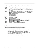
JTAG
Joint Test Action Group. A bus protocol/interface used for test and
debug.
LQFP
Low profile Quad Flat Pack
MPIO
Multi Purpose Input and Output Port on Motorola’s Family of DSPs.
Shares package pins with other peripherals on the chip and can function
as a GPIO.
OnCE
TM
On-Chip Emulation, a debug bus and port created by Motorola to enable
designers to create a low-cost hardware interface for a professional
quality debug environment.
PCB
Printed Circuit Board
PLL
Phase Locked Loop
PWM
Pulse Width Modulation
RAM
Random Access Memory
ROM
Read Only Memory
SCI
Serial Communications Interface
SPI
Serial Peripheral Interface Port on Motorola’s Family of DSPs
SRAM
Static Random Access Memory
UART
Universal Asynchronous Receiver/Transmitter
Содержание Digital DNA DSP56F807
Страница 2: ......
Страница 12: ...xii DSP56F807EVM Hardware User s Manual ...
Страница 53: ... DSP56F807EVM Schematics A 1 Appendix A DSP56F807EVM Schematics ...
Страница 72: ...A 20 DSP56F807EVM Hardware User s Manual ...
Страница 79: ......


