background image

2-2

56F805EVM Hardware User’s Manual

MOTOROLA

Connector to allow the user to connect his own SCI1 / MPIO-compatible peripheral 
[J17]

Connector to allow the user to connect his own SPI / MPIO-compatible peripheral 
[J19]

Connector to allow the user to connect his own PWMA or MPIO-compatible 
peripheral [J21]

Connector to allow the user to connect his own PWMB / MPIO-compatible 
peripheral [J22]

Connector to allow the user to connect his own CAN physical layer peripheral 
[J25]

Connector to allow the user to connect his own Timer A / MPIO-compatible 
peripheral [J3]

Connector to allow the user to connect his own Timer B / MPIO-compatible 
peripheral [J6]

Connector to allow the user to connect his own Timer C / MPIO-compatible 
peripheral [J8]

Connector to allow the user to connect his own Timer D / MPIO-compatible 
peripheral [J5]

Connector to allow the user to attach his own Port B GPIO-compatible peripheral 
[J28]

Connector to allow the user to attach his own Port D GPIO-compatible peripheral 
[J4]

Connector to allow the user to attach his own Port E GPIO-compatible peripheral 
[J7]

56F805’s external memory expansion connectors [J1, J2 and J27]

On-board power regulation from an ex12V DC-supplied power input [P2]

Light Emitting Diode (LED) power indicator [LED10]

Three on-board real-time user debugging LEDs [LED1-3]

Six on-board Primary PWM monitoring LEDs [LED4-9]

Primary UNI-3 Motor interface [J30]

— Encoder/Hall-Effect interface

— Over-Voltage sensing [U8]

— Over-Current sensing [U5]

— Phase Current sensing [U8 and U21]


F

re

e

sc

a

le

 S

e

m

ic

o

n

d

u

c

to

r,

 I


Freescale Semiconductor, Inc.

For More Information On This Product,

   Go to: www.freescale.com

n

c

.

..

Содержание 56F805

Страница 1: ...reserved 56F805 Evaluation Module Hardware User s Manual Order this document by DSP56F805EVMUM D Rev 4 06 04 2003 Freescale Semiconductor I Freescale Semiconductor Inc For More Information On This Product Go to www freescale com nc ...

Страница 2: ...Freescale Semiconductor I Freescale Semiconductor Inc For More Information On This Product Go to www freescale com nc ...

Страница 3: ...4 Clock Source 2 6 2 5 Operating Mode 2 6 2 6 Debug LEDs 2 7 2 7 Debug Support 2 7 2 7 1 JTAG Connector 2 8 2 7 2 Parallel JTAG Interface Connector 2 9 2 8 External Interrupts 2 10 2 9 Reset 2 11 2 10 Power Supply 2 11 2 11 Primary UNI 3 Interface 2 12 2 12 Secondary UNI 3 Interface 2 13 2 13 General Purpose Switches and Run Stop Switch 2 14 2 14 Serial 10 bit 4 channel D A Converter 2 15 2 15 Mot...

Страница 4: ...r Timer Channel B Expansion Connector 2 27 2 22 7 Timer Channel C Expansion Connector 2 27 2 22 8 Timer Channel D Expansion Connector 2 28 2 22 9 Address Bus Expansion Connector 2 28 2 22 10 Data Bus Expansion Connector 2 29 2 22 11 A D Port Expansion Connector 2 29 2 22 12 Serial Communications Port 0 Expansion Connector 2 30 2 22 13 Serial Communications Port 1 Expansion Connector 2 30 2 22 14 S...

Страница 5: ... 9 Run Stop and General Purpose Switches 2 14 2 10 Serial 10 bit 4 Channel D A Converter 2 15 2 11 PWM Group A Interface and LEDs 2 16 2 12 FAULTA1 Selection Circuit 2 17 2 13 DC Bus Over Voltage and Phase Over Current Detection Circuits 2 18 2 14 FAULTB1 Selection Circuit 2 19 2 15 Primary Back EMF or Motor Phase Current Sense Signals 2 20 2 16 Zero Crossing Encoder Interface 2 21 2 17 CAN Interf...

Страница 6: ...e Over Current Sense A 12 A 12 Primary Zero Crossing Quadrature Encoder or Hall Effect Selector A 13 A 13 Secondary Zero Crossing Quadrature Encoder or Hall Effect Selector A 14 A 14 Port Expansion Connectors A 15 A 15 High Speed CAN Interface A 16 A 16 Parallel JTAG Host Target Interface and JTAG Connector A 17 A 17 Power Supplies A 18 A 18 Bypass Capacitors and Spare Gates A 19 Freescale Semicon...

Страница 7: ...r 2 17 2 12 FAULTB1 Source Selection Jumper 2 19 2 13 CAN Header Description 2 22 2 14 Port B Connector Description 2 24 2 15 Port D Connector Description 2 25 2 16 Port E Connector Description 2 25 2 17 External Memory Control Signal Connector Description 2 26 2 18 Timer A Connector Description 2 26 2 19 Timer B Connector Description 2 27 2 20 Timer C Connector Description 2 27 2 21 Timer D Conne...

Страница 8: ...onnector Description 2 31 2 29 PWM Port A Connector Description 2 32 2 30 PWM Port B Connector Description 2 33 2 31 Secondary UNI 3 Unattached Signal Connector Description 2 34 Freescale Semiconductor I Freescale Semiconductor Inc For More Information On This Product Go to www freescale com nc ...

Страница 9: ...on provides an overview of the EVM and its features Chapter 2 Technical Summary describes in detail the 56F805EVM hardware Appendix A 56F805EVM Schematics contains the schematics of the 56F805EVM Appendix B 56F805EVM Bill of Material provides a list of the materials used on the 56F805EVM board Suggested Reading Documentation on the 56F805 and the 56F805EVM kit may be found at this URL http www mot...

Страница 10: ...r 10 34 Binary Values Begin with the letter b attached to the number b1010 b0011 Numbers Considered positive unless specifically noted as a negative value 5 10 Voltage is often shown as positive 3 3V Bold Reference sources paths emphasis see http www motorola com A D Analog to Digital CAN Controller Area Network a serial communications peripheral and method CiA CAN in Automation an international C...

Страница 11: ...nd Output Port shares package pins with other peripherals on the chip and can function as a GPIO OnCETM On Chip Emulation a debug bus and port created by Motorola to enable designers to create a low cost hardware interface for a professional quality debug environment PCB Printed Circuit Board PLL Phase Locked Loop PWM Pulse Width Modulation RAM Random Access Memory ROM Read Only Memory SCI Serial ...

Страница 12: ...xii 56F805EVM Hardware User s Manual MOTOROLA Freescale Semiconductor I Freescale Semiconductor Inc For More Information On This Product Go to www freescale com nc ...

Страница 13: ...e user to easily specify complex break conditions and to execute user developed software at full speed until the break conditions are satisfied The ability to examine and modify all user accessible registers memory and peripherals through the OnCE port greatly facilitates the task of the developer Serving as a platform for hardware development The hardware platform enables the user to connect exte...

Страница 14: ...fault jumper group settings 56F805 RESET MODE IRQ Address Data Control JTAG OnCE XTAL EXTAL SPI SCI 0 SCI 1 CAN TIMER GPIO PWM 1 A D PWM 2 3 3 V GND Peripheral Expansion Connector s RESET LOGIC MODE IRQ LOGIC Program Memory 64Kx16 bit Memory Expansion Connector s JTAG Connector Parallel JTAG Interface Low Freq Crystal DSub 25 Pin Data Memory 64Kx16 bit DSub 9 Pin CAN Interface Debug LEDs PWM LEDs ...

Страница 15: ...t power for Host Target Interface 1 2 JG12 Primary Encoder Input Selected 2 3 5 6 8 9 JG13 Secondary Encoder Input Selected 2 3 5 6 8 9 JG14 Primary UNI 3 3 Phase Current Sense Selected as Analog Inputs 2 3 5 6 8 9 JG15 Primary UNI 3 Phase A Over Current Selected for FAULTA1 1 2 JG16 Secondary UNI 3 Phase B Over Current Selected for FAULTB1 1 2 JG8 JG9 DSP56F805EVM JG3 1 J29 JTAG JG14 1 P3 USER S ...

Страница 16: ...pply is not plugged into a 120V AC power source 4 Connect the 2 1mm output power plug from the external power supply into P2 shown in Figure 1 3 on the 56F805EVM board 5 Apply power to the external power supply The green Power On LED LED10 will illuminate when power is correctly applied JG17 CAN termination unselected NC JG18 Use on board crystal for oscillator input 1 2 Figure 1 3 Connecting the ...

Страница 17: ...processor The main features of the 56F805EVM include 56F805 16 bit 3 3V hybrid controller operating at 80MHz U1 External fast static RAM FSRAM memory U15 configured as 64K 16 bit of program memory with 0 wait states at 70MHz 64K 16 bit of data memory with 0 wait states at 70MHz 4 Channel 10 bit Serial D A SPI for real time user data display U18 8 00MHz crystal oscillator for frequency generation Y...

Страница 18: ...tible peripheral J8 Connector to allow the user to connect his own Timer D MPIO compatible peripheral J5 Connector to allow the user to attach his own Port B GPIO compatible peripheral J28 Connector to allow the user to attach his own Port D GPIO compatible peripheral J4 Connector to allow the user to attach his own Port E GPIO compatible peripheral J7 56F805 s external memory expansion connectors...

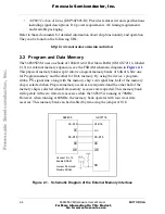
Страница 19: ...otorola DSP56F805FV80 part designated as U1 on the board and in the schematics This part will operate at a maximum speed of 80MHz A full description of the 56F805 including functionality and user information is provided in the following documents DSP56800 Family Manual DSP56800FM D Provides a detailed description of the core processor including internal status and control registers and a detailed ...

Страница 20: ...ogram memory and the other for Data memory By using the device s program strobe PS signal line along with the memory chip s A0 signal line half of the memory chip is selected when Program memory accesses are requested and the other half of the memory chip is selected when Data memory accesses are requested This memory bank will operate with zero wait state accesses while the 56F805 is running at 7...

Страница 21: ...rol is not provided but could be implemented using uncommitted GPIO signals The pinout of connector P3 is listed in Table 2 1 The RS 232 level converter transceiver can be disabled by removing the jumper at JG9 Figure 2 2 Schematic Diagram of the RS 232 Interface Table 2 1 RS 232 Serial Connector Description P3 Pin Signal Pin Signal 1 Jumper to 6 4 6 Jumper to 1 4 2 TXD 7 Jumper to 8 3 RXD 8 Jumpe...

Страница 22: ...ce 2 5 Operating Mode The 56F805EVM provides a boot up MODE selection jumper JG7 This jumper is used to select the operating mode of the device as it exits RESET Refer to the DSP56F801 803 805 807 User s Manual for a complete description of the chip s operating modes Table 2 2 shows the two operation modes available on the 56F805 Table 2 2 Operating Mode Selection Operating Mode JG7 Comment 0 1 2 ...

Страница 23: ...PB2 to a Logic One value will turn on the associated LED Figure 2 4 Schematic Diagram of the Debug LED Interface 2 7 Debug Support The 56F805EVM provides an on board Parallel JTAG Host Target Interface and a JTAG interface connector for external Target Interface support Two interface connectors are provided to support each of these debugging approaches These two connectors are designated the JTAG ...

Страница 24: ...r When this connector is used with an external Host Target Interface the parallel JTAG interface should be disabled by placing a jumper in jumper block JG5 Reference Table 2 4 for this jumpers selection options Table 2 3 JTAG Connector Description J29 Pin Signal Pin Signal 1 TDI 2 GND 3 TDO 4 GND 5 TCK 6 GND 7 NC 8 KEY 9 RESET 10 TMS 11 3 3V 12 NC 13 NC 14 TRST Table 2 4 Parallel JTAG Interface Di...

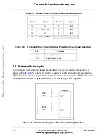
Страница 25: ...get Interface to be powered by the Target board instead of the Host system when necessary reference Table 2 6 This may be necessary when using a 3 3V Host computer parallel port Figure 2 5 Block Diagram of the Parallel JTAG Interface Table 2 5 Parallel JTAG Interface Connector Description P1 Pin Signal Pin Signal 1 NC 14 NC 2 PORT_RESET 15 PORT_IDENT 3 PORT_TMS 16 NC 4 PORT_TCK 17 NC 5 PORT_TDI 18...

Страница 26: ... user to generate interrupts for his user specific programs Figure 2 6 Schematic Diagram of the User Interrupt Interface 10 NC 23 GND 11 PORT_TDO 24 GND 12 NC 25 GND 13 PORT_CONNECT Table 2 6 On Board Host Target Interface Power Source Jumper Selection JG11 Comment 1 2 Host supplied power 2 3 Target supplied power Table 2 5 Parallel JTAG Interface Connector Description P1 Pin Signal Pin Signal 56F...

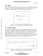
Страница 27: ...05EVM however less than 500mA is required by the EVM The remaining current is available for user motor control applications when connected to an optional motor power stage board The 56F805EVM provides 3 3V DC voltage regulation for the device memory D A CAN parallel JTAG interface and supporting logic refer to Figure 2 8 Power applied to the 56F805EVM is indicated with a Power On LED referenced as...

Страница 28: ...in Signal 1 PWM_AT 2 Shield 3 PWM_AB 4 Shield 5 PWM_BT 6 Shield 7 PWM_BB 8 Shield 9 PWM_CT 10 Shield 11 PWM_CB 12 GND 13 GND 14 5 0V DC 15 5 0V DC 16 Analog 3 3V DC 17 Analog GND 18 Analog GND 19 Analog 15V DC 20 Analog 15V DC 21 Motor DC Bus Voltage Sense 22 Motor DC Bus Current Sense 23 Motor Phase A Current Sense 24 Motor Phase B Current Sense 25 Motor Phase C Current Sense 26 Motor Drive Tempe...

Страница 29: ... and to Table 2 9 for the pin out of the unused signal header Table 2 8 Secondary UNI 3 Connector Description J31 Pin Signal Pin Signal 1 PWM_AT 2 Shield 3 PWM_AB 4 Shield 5 PWM_BT 6 Shield 7 PWM_BB 8 Shield 9 PWM_CT 10 Shield 11 PWM_CB 12 GND 13 GND 14 NC 15 NC 16 NC 17 Analog GND 18 Analog GND 19 NC 20 NC 21 Motor DC Bus Voltage Sense 22 Motor DC Bus Current Sense 23 Motor Phase A Current Sense ...

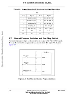
Страница 30: ... Stop and General Purpose Switches Table 2 9 Unused Secondary UNI 3 Connector Signal Description J14 Pin Signal Pin Signal 1 SU3_ZERO_X_A 2 SU3_ZERO_X_B 3 SU3_ZERO_X_C 4 SU3_BK_EMF_A 5 SU3_BK_EMF_B 6 SU3_BK_EMF_C 7 SU3_PHA_IS 8 SU3_PHB_IS 9 SU3_PHC_IS 10 SU3_I_S_DCB 11 GND 12 5 0V 13 NC 14 NC 56F805 3 3V PD3 PD4 PD5 GP SWITCH 1 GP SWITCH 2 RUN STOP SWITCH 3 3V 3 3V Freescale Semiconductor I Freesc...

Страница 31: ...utput full scale range value can be set to a value from 0 0V to 2 4V by a trimpot This trimpot is preset to 2 05V which provides approximately 2mV per step Figure 2 10 Serial 10 bit 4 Channel D A Converter Table 2 10 D A Header Description J20 Pin Signal Pin Signal 1 D A Channel 0 2 AGND 3 D A Channel 1 4 AGND 5 D A Channel 2 6 AGND 7 D A Channel 3 8 AGND 56F805 U18 D A CONNECTOR MOSI MISO SCLK PB...

Страница 32: ...ontains two UNI 3 connectors that interface with various motor drive boards Primary UNI 3 and Secondary UNI 3 The device can sense error conditions generated by the motor power stage boards via signals on the UNI 3 connector The motor driver board s Motor Supply DC Bus Voltage Current and Motor Phase Currents are sensed on the power stage board The conditioned signals are transferred to the board ...

Страница 33: ...Over Current circuit for the UNI 3 interface The FAULTA1 input can be sourced from the Phase A Over Current circuit or the DC Bus Over Current circuit Jumper JG15 provides the selection see Figure 2 12 and Table 2 11 Figure 2 12 FAULTA1 Selection Circuit Table 2 11 FAULTA1 Source Selection Jumper JG15 Comment 1 2 Phase A Over Current Sense input 2 3 DC Bus Over Current Sense input DC BUS CURRENT S...

Страница 34: ...TB1 FAULTB2 and FAULTB3 The Secondary UNI 3 interface is similar to the circuits contained in Figure 2 13 The FAULTB1 input can be sourced from the Phase A Over Current circuit or the DC Bus Over Current circuit Jumper JG16 provides the selection reference Figure 2 14 and Table 2 12 Figure 2 13 DC Bus Over Voltage and Phase Over Current Detection Circuits 5 0V 5 0V 3 3V V_sense_DCB FAULT0 LM393 5 ...

Страница 35: ...umper JG16 Comment 1 2 Phase A Over Current Sense input 2 3 DC Bus Over Current Sense input DC BUS CURRENT SENSE I_sense_DCB 5 0V 5 0V 3 3V 3 2 1 5 0V 3 3V 5 0V PHA_IS LM393 LM393 PHASE A CURRENT SENSE FAULTB1 JG16 Freescale Semiconductor I Freescale Semiconductor Inc For More Information On This Product Go to www freescale com nc ...

Страница 36: ... can exceed this maximum range The Motor Phase Current signals are derived from current sense resistors Both of these signal groups are then routed to a group of header pins that allow the end user to select which signal group the device s A D will monitor Refer to Figure 2 15 for the design of a single channel The Secondary UNI 3 s Back EMF signals are unbuffered and then routed to a header that ...

Страница 37: ...ic that can send out pulses when the phase voltage of an attached 3 phase motor drops to zero The motor drive board circuits generate a 0 to 3 3V DC pulse via voltage comparators The resulting pulse signals are sent to a set of jumper blocks shared with the Encoder Hall Effect interface The jumper blocks allow the selection of Zero Crossing signals or Quadrature Encoder Hall Effect signals When in...

Страница 38: ...y chaining of CAN devices CAN bus termination of 120 ohms can be provided by adding a jumper to JG17 Refer to Table 2 13 for the CAN connector signals and Figure 2 17 for a connection diagram Figure 2 17 CAN Interface Table 2 13 CAN Header Description J26 and J32 Pin Signal Pin Signal 1 NC 2 NC 3 CANL 4 CANH 5 GND 6 NC 7 NC 8 NC 9 NC 10 NC 56F805 MSCAN_TX MSCAN_RX CAN CONNECTOR TXD RXD SLOPE VREF ...

Страница 39: ...ftware Feature Jumpers 2 22 Peripheral Connectors The EVM board contains a group of Peripheral Expansion Connectors used to gain access to the resources of the 56F805 The following signal groups have Expansion Connectors Port B Port D Port E External Memory Control Encoder A Timer Channel A Encoder B Timer Channel B Timer Channel C Timer Channel D Port A Address Bus Data Bus A D Input Port Serial ...

Страница 40: ...re dedicated to general purpose I O and Interrupt operations The GPIO port pins may be programmed as inputs outputs or level sensitive interrupt inputs Table 2 14 shows the port pin to headed connections Table 2 14 Port B Connector Description J28 Pin Signal Pin Signal 1 PB0 2 PB1 3 PB2 4 PB3 5 PB4 6 PB5 7 PB6 8 PB7 9 GND 10 3 3V Freescale Semiconductor I Freescale Semiconductor Inc For More Infor...

Страница 41: ...le 2 22 2 22 3 Port E Expansion Connector Port E is an MPIO port with signal lines attached to various headers The pins of the port are shared with one SCI port SCI0 two Address bus lines A6 and A7 and the SPI port Table 2 16 shows the shared pins and functions Table 2 15 Port D Connector Description J4 Pin Signal Pin Signal 1 PD0 2 PD1 3 PD2 4 PD3 5 PD4 6 PD5 7 GND 8 3 3V Table 2 16 Port E Connec...

Страница 42: ... Timer A expansion connector The port can act as a Quadrature Decoder interface port or as a general purpose Timer port See to Table 2 18 for the signals attached to the connector Table 2 17 External Memory Control Signal Connector Description J27 Pin Signal Pin Signal 1 RD 2 IRQA 3 WR 4 IRQB 5 PS 6 RESET 7 DS 8 RSTO 9 CLKO 10 DE 11 GND 12 3 3V Table 2 18 Timer A Connector Description J3 Pin Signa...

Страница 43: ...ached to the connector 2 22 7 Timer Channel C Expansion Connector The Timer Channel C port is an MPIO port attached to the Timer C expansion connector Refer to Table 2 20 for the signals attached to the connector Table 2 19 Timer B Connector Description J6 Pin Signal Alternate 1 TB0 PhaseA1 2 TB1 PhaseB1 3 TB2 INDEX1 4 TB3 HOME1 5 3 3V 3 3V 6 GND GND Table 2 20 Timer C Connector Description J8 Pin...

Страница 44: ...ry address signal lines The upper 8 bits A8 A15 can also be used as Port A GPIO lines Refer to Table 2 22 for the Address bus connector information Table 2 21 Timer D Connector Description J5 Pin Signal 1 TD0 2 TD1 3 TD2 4 TD3 5 3 3V 6 GND Table 2 22 External Memory Address Bus Connector Description J1 Pin Signal Pin Signal 1 A0 2 A1 3 A2 4 A3 5 A4 6 A5 7 A6 8 A7 9 A8 10 A9 11 A10 12 A11 13 A12 14...

Страница 45: ...ersion port is attached to this connector See Table 2 24 for connection information Table 2 23 External Memory Address Bus Connector Description J2 Pin Signal Pin Signal 1 D0 2 D1 3 D2 4 D3 5 D4 6 D5 7 D6 8 D7 9 D8 10 D9 11 D10 12 D11 13 D12 14 D13 15 D14 16 D15 17 GND 18 3 3V Table 2 24 A D Connector Description J9 Pin Signal Pin Signal 1 AN0 2 AN4 3 AN1 4 AN5 5 AN2 6 AN6 7 AN3 8 AN7 9 GNDA 10 3 ...

Страница 46: ... Serial Communications Port 1 Expansion Connector The Serial Communications Port 1 SCI1 is attached to this connector Refer to Table 2 26 for connection information Table 2 25 SCI0 Connector Description J16 Pin Signal 1 TXD0 2 RXD0 3 GND Table 2 26 SCI1 Connector Description J17 Pin Signal 1 TXD1 2 RXD1 3 GND Freescale Semiconductor I Freescale Semiconductor Inc For More Information On This Produc...

Страница 47: ... information 2 22 15 CAN Expansion Connector The CAN port is attached to this connector Refer to Table 2 28 for connection information Table 2 27 SPI Connector Description J19 Pin Signal 1 MOSI 2 MISO 3 SCLK 4 GND Table 2 28 CAN Connector Description J25 Pin Signal 1 MSCAN_TX 2 MSCAN_RX 3 GND Freescale Semiconductor I Freescale Semiconductor Inc For More Information On This Product Go to www frees...

Страница 48: ...o Table 2 29 for the connection information Table 2 29 PWM Port A Connector Description J21 Pin Signal 1 ISA0 2 ISA1 3 ISA2 4 FAULTA0 5 FAULTA1 6 FAULTA2 7 FAULTA3 8 PWMA0 9 PWMA1 10 PWMA2 11 PWMA3 12 PWMA4 13 PWMA5 14 GND Freescale Semiconductor I Freescale Semiconductor Inc For More Information On This Product Go to www freescale com nc ...

Страница 49: ...r to Table 2 30 for the connection information Table 2 30 PWM Port B Connector Description J22 Pin Signal 1 ISB0 2 ISB1 3 ISB2 4 FAULTB0 5 FAULTB1 6 FAULTB2 7 FAULTB3 8 PWMB0 9 PWMB1 10 PWMB2 11 PWMB3 12 PWMB4 13 PWMB5 14 GND Freescale Semiconductor I Freescale Semiconductor Inc For More Information On This Product Go to www freescale com nc ...

Страница 50: ... has a total of eight test points Four test points are located near the breadboard area 3 3VA AGND 3 3V and GND Four test points are located near the Primary UNI 3 connector J30 15VA GND 15VA and GND Table 2 31 Secondary UNI 3 Unattached Signal Connector Description J14 Pin Signal Pin Signal 1 SU3_ZERO_X_A 2 SU3_ZERO_X_B 3 SU3_ZERO_X_C 4 SU3_BK_EMF_A 5 SU3_BK_EMF_B 6 SU3_BK_EMF_C 7 SU3_PHA_IS 8 SU...

Страница 51: ...MOTOROLA 56F805EVM Schematics A 1 Appendix A 56F805EVM Schematics Freescale Semiconductor I Freescale Semiconductor Inc For More Information On This Product Go to www freescale com nc ...

Страница 52: ...ISO MSCAN_RX RSTO TC0 TC1 TD0 TD1 TD2 TD3 TXD0 TXD1 SCLK CLKO EXTAL MOSI MSCAN_TX PWMB1 PWMB2 PWMB3 PWMB5 ISB1 ISB2 FAULTB0 PHASEA0 PHASEB0 INDEX0 HOME0 PHASEA1 PHASEB1 INDEX1 HOME1 FAULTB3 AN0 AN3 AN4 AN5 AN6 AN7 AN1 FAULTB1 FAULTB2 PWMB4 PWMA1 PWMA2 PWMA5 ISA1 ISA0 ISA2 FAULTA0 FAULTA3 FAULTA1 FAULTA2 PWMA0 PWMA4 PWMA3 PB0 PB1 PB2 PB3 PB4 PB6 PB7 PD2 PD3 PD4 PD5 AN2 PWMB0 SS TDO TCK TMS TDI TRST...

Страница 53: ...3 Wireless Subscriber Division 6 5 0 1 William Cannon Drive West Austin TX 78735 8598 512 895 3230 FAX 512 895 4556 MD OE314 Title Size Document N u m ber Date Designer Rev Sheet of R E S E T I R Q A I R Q B E X T B OOT E X T AL XTAL 3 3 V 3 3 V 3 3 V J G 6 1 2 3 Y 1 8 0 0 M H z S 3 S 1 S 2 C 4 4 0 1 u F C 4 6 0 1 u F R 4 8 1 0 K R 4 6 1 0 K R 4 4 1 0 K R 4 5 1 0 M J G 7 1 2 J G 1 8 1 2 Freescale ...

Страница 54: ... D 1 5 D 1 1 D 3 D 1 0 D 1 D 7 D 1 2 D 9 D 8 D 1 4 A 1 5 A 1 1 A 1 A 1 2 A 1 0 A 3 A 1 4 A 5 A 9 A 6 A 8 A 0 A 7 A 1 3 A 2 A 4 R D W R D 0 1 5 A 0 15 P S 3 3 V 3 3 V U 1 5 G S 7 2 1 1 6 T P 1 2 D Q 1 7 D Q 2 8 A 4 1 D Q 3 9 D Q 4 1 0 A 3 2 D Q 5 1 3 D Q 6 1 4 A 2 3 D Q 7 1 5 D Q 8 1 6 A 1 4 D Q 9 2 9 D Q 1 0 3 0 A 0 5 D Q 1 1 3 1 D Q 1 2 3 2 A 1 5 1 8 D Q 1 3 3 5 D Q 1 4 3 6 A 1 4 1 9 D Q 1 5 3 7 ...

Страница 55: ... I N T 2 I N T 3 I N T 3 I N E N T 2 I N T X D 0 R X D 0 3 3 V 3 3 V J G 9 1 2 R 5 5 1 K R 1 0 1 1 K R 1 0 2 1 K R 5 3 1 K R 5 2 1 K P 3 5 9 4 8 3 7 2 6 1 C 4 8 0 1 u F C 5 0 0 1 u F C 4 7 0 1 u F C 4 9 0 1 u F R 5 0 1 K R 5 1 1 K R 1 0 0 1 K C 5 1 0 1 u F U 1 6 A D M 3 3 1 1 E A R S V 1 C 2 2 V C C 3 C 2 4 E N 5 C 1 6 T 1 I N 7 T 2 I N 8 T 3 I N 9 R 1 O U T 1 0 R 2 O U T 1 1 R 3 O U T 1 2 R 4 O U...

Страница 56: ...14 Title Size Document N u m ber Date Designer Rev Sheet of D A 3 D A 2 D A 1 D A 0 Vref M I S O S C L K M O S I P B 4 R S T O 3 3 V 3 3 V 3 3 V A Vref R 5 7 5 1 K U 1 8 M A X 5 2 5 1 B E AP A G N D 1 F B A 2 O U T A 3 O U T B 4 F B B 5 R E F A B 6 R E F C D 1 5 F B C 1 6 O U T C 1 7 O U T D 1 8 F B D 1 9 V D D 2 0 U P 0 1 3 D I N 9 D O U T 1 2 S C L K 1 0 C S 8 C L 7 P D L 1 4 D G N D 1 1 J 2 0 1...

Страница 57: ...t N u m ber Date Designer Rev Sheet of P W M A 4 P W M A 1 P W M A 0 P W M A 5 P W M A 2 P W M A 3 P B 0 P B 1 P B 2 3 3 V 3 3 V L E D 4 L E D 5 L E D 6 L E D 7 L E D 8 L E D 9 L E D 1 L E D 2 L E D 3 R 5 8 2 7 0 R 5 9 2 7 0 R 6 0 2 7 0 R 6 1 2 7 0 R 6 2 2 7 0 R 6 3 2 7 0 R 6 4 2 7 0 R 6 5 2 7 0 R 6 6 2 7 0 U 1 1 F 7 4 A C 0 4 1 3 1 2 U 1 1 E 7 4 A C 0 4 1 1 1 0 U 1 1 D 7 4 A C 0 4 9 8 U 1 9 A 7 4...

Страница 58: ... 8 0 5 EVM DSN Tuesday July 04 2000 Development Tools 18 7 1 3 Wireless Subscriber Division 6 5 0 1 William Cannon Drive West Austin TX 78735 8598 5 1 2 8 9 5 3 2 3 0 F A X 5 1 2 8 9 5 4 5 5 6 MD OE314 Title Size D o c u ment N u mber D a t e D e s i g n er R e v S h e e t of PFC_PWM PFC_ZERO_CROSS SERIAL_COMM PFC_INHIBIT PFC_ZERO_CROSS PFC_PWM SERIAL_COMM PFC_INHIBIT AN0 UNI_3_ 15 UNI_3_ 15 UNI_3...

Страница 59: ... 1 3 Wireless Subscriber Division 6 5 0 1 William Cannon Drive West Austin TX 78735 8598 5 1 2 8 9 5 3 2 3 0 F A X 5 1 2 8 9 5 4 5 5 6 MD OE314 Title Size D o c u ment N u mber D a t e D e s i g n er R e v S h e e t of SU3_V_S_DCB SU3_BK_EMF_A SU3_BK_EMF_C SU3_BK_EMF_B SU3_PFC_PWM SU3_PFC_ZERO_CROSS SU3_SERIAL_COMM SU3_PFC_INHIBIT SU3_PFC_ZERO_CROSS SU3_PFC_PWM SU3_SERIAL_COMM SU3_PFC_INHIBIT SU3_...

Страница 60: ...opment Tools 18 9 1 3 Wireless Subscriber Division 6 5 0 1 William Cannon Drive West Austin TX 78735 8598 512 895 3230 FAX 512 895 4556 MD OE314 Title Size Document N u m ber Date Designer Rev Sheet of P D 3 P D 4 P D 5 P D 0 P D 1 3 3 V 3 3 V 3 3 V R 4 2 1 0 K R 7 2 1 0 K R 7 3 1 0 K R 7 4 1 0 K S 4 S 5 S 6 S W S P S T J G 1 1 2 3 R 1 1 9 1 0 K R 4 3 1 0 K J G 2 1 2 3 R 1 2 0 1 0 K Freescale Semi...

Страница 61: ...M DSN Tuesday July 04 2000 Development Tools 18 10 1 3 Wireless Subscriber Division 6 5 0 1 William Cannon Drive West Austin TX 78735 8598 512 895 3230 FAX 512 895 4556 MD OE314 Title Size Document N u m ber Date Designer Rev Sheet of B K _ E M F _ B B K _ E M F _ C S U 3 _ T E M P U 3 _ P H A _ I S A N 2 U 3 _ P H B _ I S A N 3 U 3 _ P H C _ I S A N 4 B K _ E M F _ A J G 1 4 A 1 2 3 J G 1 0 1 J G...

Страница 62: ...e s i g n er R e v S h e e t of S_PHA_IS PRI_OVER_I_LIMIT P_PHA_IS U3_I_LIMIT_REF U3_I_LIMIT_REF U3_I_LIMIT_REF SU3_I_LIMIT_REF SU3_I_LIMIT_REF SU3_I_LIMIT_REF P_PHA_IS P_OI_FAULT SEC_OVER_I_LIMIT S_PHA_IS S_OI_FAULT FAULTA3 FAULTA2 FAULTB3 FAULTB2 AN1 FAULTA1 U3_PHA_IS U3_PHB_IS U3_PHC_IS SU3_PHA_IS SU3_PHB_IS SU3_PHC_IS SU3_I_S_DCB FAULTB1 3 3V 5 0V 3 3V 3 3V 3 3V 3 3V 3 3V 5 0V 5 0V 5 0V 3 3V 5...

Страница 63: ...illiam Cannon Drive West Austin TX 78735 8598 512 895 3230 FAX 512 895 4556 MD OE314 Title Size Document N u m ber Date Designer Rev Sheet of H O M E 0 Z E R O _ X _ C Z E R O _ X _ B Z E R O _ X _ A I N D E X 0 P H A S E B 0 P H A S E A 0 5 0 V 5 0 V 5 0 V 5 0 V 5 0 V J G 1 2 A 1 2 3 R 8 6 2 4 O h m C 5 8 4 7 0 p F R 8 5 2 4 O h m R 8 4 1 K R 8 3 2 4 O h m R 8 2 2 4 O h m R 8 1 1 K C 5 7 4 7 0 p ...

Страница 64: ... 0 1 William Cannon Drive West Austin TX 78735 8598 512 895 3230 FAX 512 895 4556 MD OE314 Title Size Document N u m ber Date Designer Rev Sheet of H O M E 1 S U 3 _ Z E R O _ X _ C S U 3 _ Z E R O _ X _ B S U 3 _ Z E R O _ X _ A P H A S E A 1 P H A S E B 1 I N D E X 1 5 0 V 5 0 V 5 0 V 5 0 V 5 0 V R 9 5 2 4 O h m R 9 4 2 4 O h m R 9 3 1 K C 6 3 4 7 0 p F R 9 2 2 4 O h m R 9 1 2 4 O h m R 9 0 1 K ...

Страница 65: ... PD3 PD5 DS RSTO IRQB RESET IRQA WR RD PS RXD1 SS TXD0 RXD0 SCLK MISO MOSI TXD1 CLKO TD3 TD2 TD1 TC0 TC1 DEBUG_EVENT PHASEA1 PHASEB1 INDEX1 HOME1 TD0 PHASEA0 PHASEB0 INDEX0 HOME0 AN0 AN1 AN2 AN3 AN4 AN5 AN6 AN7 A 0 15 A 0 15 D 0 15 D 0 15 MOSI MISO SCLK ISB0 ISB1 ISB2 FAULTB0 FAULTB1 FAULTB2 FAULTB3 PWMB0 PWMB1 PWMB2 PWMB3 PWMB4 PWMB5 FAULTA1 PWMA5 FAULTA0 ISA0 PWMA0 ISA2 PWMA1 PWMA4 PWMA2 FAULTA3...

Страница 66: ...e West Austin TX 78735 8598 512 895 3230 FAX 512 895 4556 MD OE314 Title Size Document N u m ber Date Designer Rev Sheet of C A N H C A N L C A N H C A N L C A N H C A N L M S C A N _ T X M S C A N _ R X 5 0 V 5 0 V J 2 6 1 3 5 7 9 2 4 6 8 1 0 U 2 0 P C A 8 2 C 2 5 0 T TXD 1 R X D 4 G N D 2 V C C 3 V R E F 5 C A N L 6 C A N H 7 S L O P E 8 R 9 9 1 K J 3 2 1 3 5 7 9 2 4 6 8 1 0 J G 1 7 1 2 R 1 1 8 ...

Страница 67: ...ECT PORT_RESET PORT_TMS PORT_TCK PORT_IDENT PORT_VCC PORT_TDI PORT_TRST TDO TMS TCK TDI P_RESET TRST P_RESET RESET TRST TDO RESET TDI TDO TCK TMS TRST 3 3V 3 3V 3 3V 3 3V 3 3V 3 3V R33 51 Ohm R37 5 1K Q1 2N2222A R35 5 1K U9 MC74HC244DW 1Y1 18 1Y2 16 1Y3 14 1Y4 12 2Y1 9 2Y2 7 2Y3 5 2Y4 3 2G 19 1G 1 1A1 2 1A2 4 1A3 6 1A4 8 2A1 11 2A2 13 2A3 15 2A4 17 VCC 20 GND 10 R34 51 Ohm P1 DB25M 1 3 2 15 14 16 ...

Страница 68: ...e West Austin TX 78735 8598 5 1 2 8 9 5 3 2 3 0 F A X 5 1 2 8 9 5 4 5 5 6 MD OE314 Title Size D o c u ment N u mber D a t e D e s i g n er R e v S h e e t of 5 0V 3 3V 3 3V 3 3VA 5 0V 5 0V_UNI3 3 3VA 3 3V LED10 GREEN LED R40 470 P2 1 3 2 C12 0 1uF D2 FM4001 C14 0 1uF U13 MC33269DT_3 3 VIN 3 VOUT 2 VOUT 4 GND 1 U12 MC33269DT_5 0 VIN 3 VOUT 2 VOUT 4 GND 1 L1 FERRITE BEAD L4 FERRITE BEAD L2 FERRITE B...

Страница 69: ... 3 0 F A X 5 1 2 8 9 5 4 5 5 6 MD OE314 Title Size D o c u ment N u mber D a t e D e s i g n er R e v S h e e t of 3 3V 3 3V 3 3V 5 0V 3 3V Vref 3 3V 3 3VA 3 3V 3 3V 3 3V 3 3VA 3 3V 3 3V 3 3V 5 0V 5 0V 5 0V 5 0V 5 0V 5 0V 3 3V C40 0 1uF C70 0 1uF C39 0 1uF C69 0 1uF C26 0 1uF C24 0 1uF C38 0 1uF C27 0 1uF C28 0 1uF R41 5 1k C35 0 1uF C21 0 1uF C31 0 1uF C68 0 1uF C67 0 1uF C25 0 1uF C32 0 1uF C20 ...

Страница 70: ...A 20 56F805EVM Hardware User s Manual MOTOROLA Freescale Semiconductor I Freescale Semiconductor Inc For More Information On This Product Go to www freescale com nc ...

Страница 71: ...311EARS U16 Analog Devices ADM3311EARS 1 MAX5251BEAP U18 Maxim MAX5251BEAP 1 PCA82C250T U20 Philips Semiconductor PCA82C250T Resistors 20 16K Ω R1 R2 R6 R7 R9 R10 R16 R17 R20 R21 R24 R25 R28 R29 R67 R68 R108 R109 R111 R112 SMEC RC73L2A16KOHMJT 10 1M Ω R3 R8 R11 R18 R22 R26 R30 R69 R110 R113 SMEC RC73L2A1MOHMJT 21 5 1K Ω R4 R12 R13 R19 R23 R27 R31 R32 R35 R37 R41 R57 R70 R105 R106 R114 R115 R121 R1...

Страница 72: ...9 R91 R92 R94 R95 R97 R98 SMEC RC73L2A24OHMJT 1 120 Ω 1 4W R118 YAGEO CFR 120QBK Potentioneters 7 10K Ω R5 R14 R15 R71 R107 R116 R117 BC MEPCOPAL ST4B103CT Inductors 4 1 0mH L1 L2 L3 L4 Fair Rite 2743015112 LEDs 1 Red LED LED1 Hewlett Packard HSMS C650 4 Yellow LED LED2 LED4 LED6 LED8 Hewlett Packard HSMY C650 5 Green LED LED3 LED5 LED7 LED9 LED10 Hewlett Packard HSMG C650 Diode 3 S2B FM401 D1 D2 ...

Страница 73: ... JG4 J4 J20 SAMTEC TSW 104 08 S D 6 1 2 Bergstick JG5 JG7 JG8 JG9 JG17 JG18 SAMTEC TSW 102 08 S S 1 1 x 1 Bergstick JG10 SAMTEC TSW 101 08 S S 3 3 x 3 Bergstick JG12 JG13 JG14 SAMTEC TSW 103 07 S T 2 9 x 2 Bergstick J1 J2 SAMTEC TSW 109 08 S D 3 6 x 1 Bergstick J3 J5 J6 SAMTEC TSW 106 08 S S 5 5 x 2 Bergstick J7 J9 J26 J28 J32 SAMTEC TSW 105 08 S D 2 4 x 1 Bergstick J8 J19 SAMTEC TSW 104 08 S S 2 ...

Страница 74: ... P2 Switch Craft RAPC 722 1 DE9F Connector P3 AMPHENOL 617 C009S AJ120 Switches 5 SPST Pushbutton S1 S2 S3 S4 S5 Panasonic EVQ QS205K 1 SPDT Toggle S6 C K GT11MSCKE Transistors 1 2N2222A Q1 ZETEX FMMT2222ACT Miscellaneous 27 Shunt SH1 SH27 Samtec SNT 100 BL T 6 Rubber Feet RF1 RF6 3M SJ5018BLKC Qty Description Ref Designators Vendor Part Freescale Semiconductor I Freescale Semiconductor Inc For Mo...

Страница 75: ...imer compatible peripheral 2 2 UNI 3 connector interface 2 12 A A D x Analog to Digital A D x B Back EMF 2 20 C CAN x bus termination 2 1 bypass 2 1 interface 2 1 2 22 CAN in Automation CiA x CiA x Connector A D 2 29 Address bus 2 28 CAN 2 31 Data bus 2 29 External Memory Control 2 26 PWM 2 32 SCI 2 30 SPI 2 31 Connectors Peripheral Expansion 2 23 Controller Area Network CAN x D D A x D A converte...

Страница 76: ... 2 1 Motor Phase Current 2 20 Motor Protection Logic 2 16 MPIO xi 2 25 2 27 port 2 27 2 28 Multi Purpose Input and Output MPIO xi O OnCE xi 1 1 OnCE TM 1 1 On Chip Emulation OnCE xi P PCB xi Peripheral Connectors 2 23 Phase Locked Loop PLL xi PLL xi Printed Circuit Board PCB xi Program memory 2 4 Pulse Width Modulation PWM xi PWM xi Q Quad Encoder 2 21 Quadrature Decoder interface port 2 26 R RAM ...

Страница 77: ...2 12 DC Bus Over Voltage signal 2 17 Motor Drive interface 2 13 Motor interface Primary 2 2 Secondary 2 3 Over Voltage signal 2 18 Unattached Signal Connector 2 34 Universal Asynchronous Receiver Transmitter UART xi Z Zero Crossing circuits 2 21 Zero Crossing Detection 2 21 Freescale Semiconductor I Freescale Semiconductor Inc For More Information On This Product Go to www freescale com nc ...

Страница 78: ...ications can and do vary in different applications and actual performance may vary over time All operating parameters including Typicals must be validated for each customer application by customer s technical experts Motorola does not convey any license under its patent rights nor the rights of others Motorola products are not designed intended or authorized for use as components in systems intend...

Отзывы: