background image

MOTOROLA CONFIDENTIAL - PROPRIETARY

6881036B20

  November 20, 2000 

49

Level 3 Service Manual

Troubleshooting

000796-O

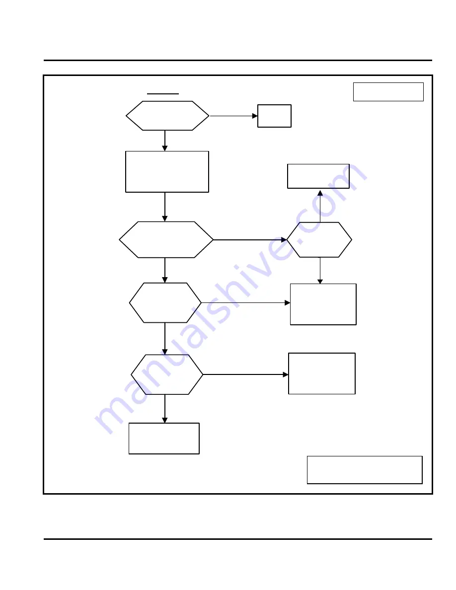
Figure 35. Frequency Error

Rephasing the phone 

using Gate22.

Is It OFF frequency ?

START

END

In test mode digit 982#, 

110062#, 1215#, 41#.

Is there noise on 

continiuos TX frequency

Check 

U350

U200


Note 1 or Faulty.

Check the presence and the 

correct value of:

 VREF on C919 from 

U900

,

RF__V1 on C217 from 

Q201

 RF___V2 on C215 from 

Q202

Check 

U200

 Note 1 or 

Faulty.

YES

NO

NO

YES

Is there noise on 

C225

 (13Mhz) ?

Check 

CR248

, relative 

components, and 

U200


Note 1 or Faulty.

Is the frequency 

on 

C225 

13 Mhz? 

Check 

Y200

 then 

U200


Note 1 or Faulty.

YES

YES

YES

NO

NO

NO

Is the frequency 

on 

R2477 

26 Mhz? 

Note 1: Check components for correct 
orientation, cold solder joints, physical 

damage, and functionallity.

In most cases, use a test 
PCB as a reference.

Содержание 38C V100

Страница 1: ...Level 3 Service Manual Model V100 GSM Technology Product Family 38C Personal Communicator ...

Страница 2: ......

Страница 3: ...Warranty Service Policy 3 General Operation 5 Operating Power 6 Nonvolatile Memory Memory Retention 6 Circuit Description 7 Overview 7 Transceiver 9 Controller 14 Troubleshooting 23 Tools and Test Equipment 23 GSM Test Commands 25 Programming Software Upgrade and Flexing 26 Troubleshooting Charts 27 Part Number Charts 53 Model Chart 53 Identity and Security 57 Related Publications 59 Exploded View...

Страница 4: ...MOTOROLA CONFIDENTIAL PROPRIETARY ii November 20 2000 6881036B20 Table of Contents Product Family 38C ...

Страница 5: ...e front cover Product names are subject to change without notice Some product names as well as some frequency bands are available only in certain markets Product Changes When electrical mechanical or production changes are incorporated into Motorola paging products a revision letter is assigned to the chassis or kit affected for example A B or C and so on The chassis or kit number complete with re...

Страница 6: ...is regard you may not use the information in this manual to create a software application for separate sale or license to others not in connection with the associated product purchased from Motorola Inc About This Service Manual Using this service manual and the many suggestions contained in it assures proper installation operation and maintenance of Product Family 38C Personal Communicators Refer...

Страница 7: ... will be sold with the standard 12 months warranty terms and condi tions Accidental damage misuse and extended warranties offered by retailers are not supported under warranty Non warranty repairs are available at agreed fixed repair prices Out of Box Failure Policy The standard out of box failure criteria applies Customer units that fail very early on after the date of sale are to be returned to ...

Страница 8: ... 3 limited PCB component The Motorola Hi Tech Centers will perform level 4 full component repairs Customer Support Customer support is available through dedicated Call Centers and in country help desks Product Service training should be arranged through the local Motorola Support Center Ordering Replacement Parts Only centers authorized to carry out repairs can purchase spare parts Orders for spar...

Страница 9: ...y LiquidCrystal Display LCD and alert tones The controller processes coded messages and forwards the messages to the trans mitter The transmitter section generates a modulated RF carrier signal amplifies the signal then radiates the signal through the antenna The following describes the general theory of operation for the Product Family 38C Personal Communicator See Figure 1 for a simplified high ...

Страница 10: ...setup information stored in FLASH memory are maintained after removing the primary battery from the device E There is a danger of explosion if the Lithium Ion battery pack is replaced incorrectly Replace only with the same type of battery or equivalent as recommended by the battery manufacturer Dispose of used batteries according to the manufacturer s instructions To ensure proper memory retention...

Страница 11: ...ter that provides additional selectivity before being fed to the Mixer A received PCS signal initially follows the same path as GSM The output from the RF switch is filtered to allow only PCS signals to pass then fed to the PCS switch The switch routes the PCS signal to a low noise amplifier A second provides additional selectivity before passing to the mixer The dual transistor mixer is split bet...

Страница 12: ...y presence and measures its temperature and voltage Charger presence and type are also sensed the keypad and display backlights are turned on and the 13 MHz clock is started The SIM subscriber identity module interface is part of the Whitecap IC and supports both synchronous prepay card and asynchronous serial data transmis sion as well as both 3V and 5V cards The charger is capable of supplying t...

Страница 13: ... through FL1400 The PCS 1900 and DCS 1800 signals are fed to DCS PCS select switch U400 RVCO_PCS and RVCO_DCS Q1100 then selects the appropriate signal with output tuning provided by L1411 and C1411 for DCS and C2411 for PCS The selected signal is fed to a low noise amplifier circuit Since this circuit is critical for achieving a very low signal to noise ratio a large amount of external frequency ...

Страница 14: ...d internally to base band digital form and passed along the RX SPI bus to the Whitecap IC The RX SPI signal is made up of BDR base band data receive BFSR Base band Frame Synch Receive and BCLKR base band clock receive fed from Magic IC Pin G8 Pin G9 and Pin F7 respectively The Whitecap IC U800 receives these signals on Pin A3 Pin D4 and Pin B4 Within the Whitecap IC the signal is digitally process...

Страница 15: ...Whitecap IC to Magic IC on TX SPI bus BDX Within the Magic IC each bit of data is clocked into a register The clocked bit and the three preceding bits on the register are then clocked into a look up ROM which looks at the digital word and from that information downloads the appropriate GSMK digital representation Channel information and AFC information from Magic IC SPI is then added to this new d...

Страница 16: ...urn creates V1_FILT The TX VCO IC produces the required output frequency and is controlled by TX_DCS TX275 DCS_SEL through Q1101 TX275_GSM GSM_SEL RX275 Q110 TX275_DPCS GSM_SEL RX275 Q2102 These signals configure the VCO for correct mode of operation GSM 900 1800 1900 support voltage being SF_OUT Magic IC Pin C1 The TX VCO signal is then fed through buffer amplifier Q330 which is supported by TX27...

Страница 17: ... U390 controls the power output of the transmitter Below is a list of the main signals associated with the PAC IC and their function RF detector RF_IN U390 Pin 2 provides a DC level proportional to the peak RF voltage out of the power amplifier RF_IN is taken via an inductively cou pled stripline at the output of the PA DET_SW U390 Pin 11 controls the variable gain stage connected between the RF d...

Страница 18: ... Power from the battery is taken from BATT battery contacts J604 and routed through battery FET Q901 Once B is available the unit carries out the following checks Battery temperature is measured to establish whether rapid charge is required Table 2 shows voltages appearing at BATT_THERM_AD J604 Pin 3 and GCAP II Pin B3 for various battery temperatures Presence and type of charger is sensed MANTEST...

Страница 19: ...775V is available whenever the radio is on and supplies most of the logic side of the board V2 is supplied from of GCAP II Pin J2 and can be measured at either C939 or C941 V3 Programmed to 2 003V to support the Whitecap IC but does not support the normal 2 75V logic output from the Whitecap IC V3 originates from GCAP II Pin B5 and can be measured at C909 or C910 VSIM1 Used to power either 3V or 5...

Страница 20: ... See also Charger Circuit on page 18 The power up sequence continues as shown in Figure 8 On initial power up all the keypad backlights DS500 DS509 and DS512 DS522 and display backlights DS504 DS510 on the antenna board in flip housing are turned on They are supported by the signal ALRT_VCC B through Q903 and switched by BKLT_EN Whitecap IC Pin K3 through Q907 000720 O Figure 8 Power up Sequence T...

Страница 21: ...1 is fed to Magic IC Pin G6 This in turn switches the Multiplexer from the output of Y200 to the output of CR248 see Figure 9 SIM Card Interface The SIM interface is part of the Whitecap IC U800 and supports both synchronous prepay card and asynchronous serial data transmission The SIM card is interro gated on power up VSIM1 SIM_VCC defaults to 3V but if a 5V card is present the SIM card is powere...

Страница 22: ...T_THERM voltage approximately 2 51V but the SIM card is either not inserted or faulty CHECK CARD displays Charger Circuit Either the mid rate charger or the full rate charger may be used See also Charger Power Source on page 14 In standby Q905 is opened to provide the approximately 50mA required by the PF38C Personal Communicator circuitry Q900 also opens controlled by CHRGC GCAP II Pin E8 to prov...

Страница 23: ...mode saves battery life by intermittently shutting off part of the PCB as follows STBY_DL is generated from Whitecap IC Pin F1 through a standby delay circuit consisting of diode CR912 and logic gate U906 which provides a short delay between activation of STBY_PC5 and STBY_DL This is a hardware patch for timing issues related to the Whitecap IC s deep sleep module DSM The resulting signal is passe...

Страница 24: ...ive state high or low for columns and rows can be selected by setting bit 2 of the COL_CONTROL and ROW_CONTROL respectively In this product the keys are active low The front keys and the PCB artwork keys use a three contact design One of the contacts is tied to ground while the other two are connected to the row and column inputs When a key is pressed all three of its pads are shorted and therefor...

Страница 25: ... Whitecap IC Pin B11 to J902 Pin 4 8 Data Lines from Whitecap IC DO D7 The display is supported by V2 and 10V originating from U904 and can be measured on C965 The data command signal AO from Whitecap IC Pin B12 Vibrator Vibrator M1 is reflowed to the bottom side of the Controller board The vibrator is controlled by the signal VIB_EN Whitecap IC Pin K1 and B through U501 Z S529 0 0 Comma S528 0 0 ...

Страница 26: ...MOTOROLA CONFIDENTIAL PROPRIETARY 22 November 20 2000 6881036B20 Circuit Description Product Family 38C ...

Страница 27: ... Radial UMP Connector Extraction Tool 1 Used to disconnect the coaxial cable from the transceiver circuit board RSX4043 A Torque Driver1 Used to remove and replace screws Torque Driver Bit T 6 Plus Apex 440 6IP Torx Plus or equivalent1 Used with torque driver 6680388B67 Disassembly tool plastic with flat and pointed ends1 Used during assembly disassembly of device 6680388B01 Delrin Tweezers1 Used ...

Страница 28: ...roubleshoot device SKN4858A EMMI Box GSM RAE RJ45 BP1 Used to program Whitecap Table 6 General Test Equipment Continued Motorola Model Number Equipment Type Application 1 To order contact Motorola Aftermarket and Accessories Division at 847 538 8000 2 Not available from Motorola To order contact Hewlett Packard at 1 800 452 4844 3 Not available from Motorola To order contact Rohde Schwarz at www r...

Страница 29: ...itiate acoustic loopback 37 Stop test 38 Activate SIM 39 Deactivate SIM 43x Change audio path 47xx Set audio volume 51 Enable sidetone 52 Disable sidetone 57 Initialize non volatile memory 58 Display security code 58xxxxxx Modify security code 59 Display lock code 59xxx Modify lock code 60 Display IMEI 993 Display all display pixels 98xx Change GSM mode primary access code 20 GSM 1800 21 GSM 900 2...

Страница 30: ...881036B20 Troubleshooting Product Family 38C Programming Software Upgrade and Flexing Contact your local technical support engineer for information about equipment and equipment setup for flashing and flexing An Emmi2D box or above is required for flashing ...

Страница 31: ...Signals 16 32 No Receiver Control Matrix 17 33 No Receiver VCO 18 34 Device Will Not Transmit 19 35 Low Transmitter Power 21 37 No Transmitter Control Matrix 22 38 PIN Diode Band Select 23 39 Receiver VCO Band Select 24 40 Device Will Not Power Up 25 41 No Ring Tone 27 43 No Audio 28 44 Headset Microphone Not Functioning 29 45 No Display 30 46 Real Time Clock Not Functioning 31 47 Check Card 32 47...

Страница 32: ...nder battery power Turn UUT off Does UUT draw 1mA when off Are correct software and Flex File installed Display functions correctly Keypad functions correctly UUT displays Check Card UUT goes into service at 102 dbm in GSM mode See Figure 34 Device Draws Current When Powered Off See Figure 30 No Display See Figure 37 Keypad Not Functioning See Figure 32 Check Card See Figure 15 Device Will Not Rec...

Страница 33: ...yzer Ringer tone audible Vibrator functions correctly Answer call Is frequency error A FC ok Insert Headset See Figure 16 Device Will Not Receive DCS PCS Signals See Figure 19 Device Will Not Transmit Sheet 1 of 2 See Figure 27 No Ring Tone See Figure 39 VibraCall Not Functioning See Figure 35 Frequency Error Signals and voltages must be at the correct level and undistorted If in doubt compare wit...

Страница 34: ... correctly Real time clock functions correctly Check for intermittent faults then end See Figure 29 Headset Microphone Not Functioning See Figure 28 No Audio See Figure 38 Voice Recognition Annotation Not Functioning See Figure 38 Voice Recognition Annotation Not Functioning See Figure 31 Real Time Clock Not Functioning NO NO NO NO NO Internal Charger functions correctly See Figure 36 No Charging ...

Страница 35: ... at C480 NO YES 400 MHz signal present on C481 NO YES Check in order U200 and U800 See Note 1 Correct signal present on C405 NO YES RX275_GSM signal present on collector of Q400 No See P Figure 17 No Receiver Control Matrix Yes Check Q400 See Note 1 Correct signal present on C453 YES Check FL401 See Note 1 Correct signal present on C460 400 MHz YES RX275 signal present on Q450 Pin 1 and RX275_GSM ...

Страница 36: ...1 See L Figure 24 Receiver VCO Band Select 1960 MHz PCS signals are present on C1402 YES Check U400 See Note 1 Correct signal is present on C1405 YES RX275_DPCS is present on collector of Q1400 See Note 1 Correct signal is present on C2452 YES Check FL1401 See Note 1 400 MHz signal is present on C460 YES RX275_DPCS is present on Q450 Pin 3 approximately 1 2V See Note 1 Check for intermittent fault...

Страница 37: ...nt on Q112 Pin 4 Check U800 See Note 1 Check Q2102 See Note 1 Check Q2101 See Note 1 Check Q112 See Note 1 Check U200 See Note 1 RX275_DPCS signal is present on Q2102 Pin 2 RX275_GSM_PCS signal is present on Q2101 Pin 2 GSM_SEL and DCS_SEL signals are present on Q110 Pin 1 and Pin 3 See Note 1 RX CONTROL MATRIX functioning properly END Check U900 See Note 1 Check Q202 and U200 See Note 1 VREF sign...

Страница 38: ...O_275 present on L259 See Note 1 RVCO_275 voltage present on U250 Pin 6 Check Q1100 then U200 See Note 1 Check in order U250 U200 and U800 See Note 1 NO NO NO YES YES YES L RVCO_DCS and RVCO_PCS voltages present on U250 Pin 3 and Pin 4 NO YES Check Q1100 then U200 See Note 1 Check Q252 See Note 1 2 Is signal present on U250 Pin 1 1347 4 MHz Note 1 Check components for correct orientation cold sold...

Страница 39: ...RFCN 1215 TX level and 310 Pseudo random TX 3 A signal is present but it is low YES Transmit power is low YES Problem occurs on all bands If unit passes H tests see Figure 22 No Transmitter Control Matrix check U300 and CR300 thru CR306 See Note 1 NO NO YES NO M H C 1 Check signals on U350 Pin 6 SF_OUT from L350 U200 Pin 5 TX275_DPCS if DCS PCS channel is selected If not present see H Figure 22 No...

Страница 40: ...l from U390 is present on Q331 See Note 1 Correct signal is present on U150 Pin 1 Does unit pass H tests see Figure 22 No Transmitter Control Matrix YES NO Check U300 and CR300 thru CR306 See Note 1 NO See H Figure 22 No Transmitter Control Matrix Check Q330 and the components supporting Q331 NO Check U390 and U200 1 Check bias on U300 Pins 2 and 8 Negative control voltage from gate control If neg...

Страница 41: ...ct signal is present on U390 Pin 7 5V is present on U903 Pin1 No check U903 and U904 Yes check Q370 and R103 See Note 1 5V is present on Q370 Pin 1 Negative bias approximately 3V P P is present on U300 Pin 2 and Pin 8 1 DM_CS is present on Q381 No check U800 See Note 1 2 Correct control signal is present on Q380 Pin 4 1 Replace U300 2 Check for intermittent fault See Note 1 YES YES YES YES YES NO ...

Страница 42: ... present on C213 U900 No check U900 Yes check Q201 and U200 See Note 1 NO YES YES YES YES YES YES NO NO NO NO NO Check Q120 See Note 1 Check U200 See Note 1 Check U200 See Note 1 Check Q2120 See Note 1 Check Q121 See Note 1 TX275 is present on C1125 SFOUT is present on Q121 Pin 4 Correct signal is present on Q2120 Pin 1 Correct signal is present on C1126 near Q2120 Note 1 Check components for corr...

Страница 43: ...1 Pin 3 and Pin 1 Check U200 See Note 1 YES YES YES NO NO NO TX_GSM and TX_DCS are present on Q1101 Pin 4 and Pin 6 10V is present on C102 Check Q1101 See Note 1 Check U903 and U904 See Note 1 Check for intermittent operation See Note 1 Note 1 Check components for correct orientation cold solder joints physical damage and functionallity In most cases a reference board can be used to compare signal...

Страница 44: ...3 and Pin 1 NO NO NO YES YES YES Check Q1100 See Note 1 Check U200 and Q100 See Note 1 Check U903 and U904 See Note 1 Check for intermittent operation See Note 1 RVCO_PCS and RVCO_DCS are present on Q1100 Pin 4 and Pin 6 5V is present on R103 Note 1 Check components for correct orientation cold solder joints physical damage and functionallity In most cases a reference board can be used to compare ...

Страница 45: ... C910 V_REF 2 8V C919 1 For incorrect V_BOOST check in order L901 CR902 R904 and U900 2 For other incorrect voltages check for shorts to ground and check U900 See Note 1 26 MHz signal is present on R244 near U200 RF_V1 is present on Q201 2 7V at C217 and RF_V2 is present on Q202 2 7V at C215 No check Q201 Q202 and U200 Yes check Y200 and U200 See Note 1 13 MHz clock is present on C225 No check CR2...

Страница 46: ... 2 GCAP_CK is present on keypad test point Reset line on C820 near Remains high 1 Remove temporary short from R943 2 Check for intermittent fault 3 Send to HTC if still faulty Check U900 U701 U702 and U800 See Note 1 Check U800 See Note 1 YES NO YES A NO Note 1 Check components for correct orientation cold solder joints physical damage and functionallity ...

Страница 47: ...enter 432 change audio path 1556 generate tone 4707 set audio volume 2 7V is present on Q903 Pin 4 No check U900 Yes check Q903 See Note 1 YES YES NO NO Ring signal is present on Alert Terminal Pin ALRT_OUT Check U900 See Note 1 Check for intermittent fault at LS1 NO YES 1 Install correct software and flex file 2 Reset UUT by entering 57 3 If malfunction persists continue Approximately 3V is prese...

Страница 48: ... audio volume START 1 KHz tone approximately 0 5V P P is present on headset terminal Check J504 C511 C951 C952 and R961 See Note 1 1 Remove headset 2 2 7V is present on R977 Check J504 See Note 1 Check U900 See Note 1 1 Connect headset 2 Voltage on R977 is now approximately 0 5V Check R976 CR901 See Note 1 NO NO YES YES NO YES Note 1 Check components for correct orientation cold solder joints phys...

Страница 49: ...initiate acoustic loopback 4707 set audio level Approximately 1V is present on C1025 Check J504 U900 and related components See Note 1 Check J504 See Note 1 Check U800 and U900 See Note 1 Check R976 CR901 See Note 1 YES NO NO NO NO YES YES YES MIC signal is present on C1025 Check R928 and C927 See Note 1 YES NO 1 Remove headset 2 2 7V is present on R977 1 Connect headset 2 Approximately 0 5V is no...

Страница 50: ... flip with known good one 2 Check ZIF connector J902 For poor contrast check C702 through C706 10V is present on C965 Check U800 See Note 1 Check U903 U904 and related components See Note 1 START NO YES Still no display Replace flip NO YES Note 1 Check components for correct orientation cold solder joints physical damage and functionallity ...

Страница 51: ... 1 Note 1 Check components for correct orientation cold solder joints physical damage and functionallity 1 Place UUT into manual test mode then enter 38 activate mini SIM 2 The following signals are present on SIM connector J900 a 3V or 5V on Pin 3 VSIM1 b 3 25 MHz on Pin 1 CLK c Data signal on Pin 6 SIM_I O 1 Check for intermittent fault 2 Check in order U800 U900 See Note 1 1 VSIM1 check U900 2 ...

Страница 52: ...l damage and functionallity Check the following supply lines for any short to ground or different resistences comparing with a good PCB B on C915 V_BOOST1 on C913 V_REF on C919 V1 on C906 V2 on C939 V3 on C910 VSIM1 on C905 If you found differences check the components which use that Voltage If you don t find any difference send PCB to HTC Note 1 Check components for correct orientation cold solde...

Страница 53: ...Check the presence and the correct value of VREF on C919 from U900 RF__V1 on C217 from Q201 RF___V2 on C215 from Q202 Check U200 Note 1 or Faulty YES NO NO YES Is there noise on C225 13Mhz Check CR248 relative components and U200 Note 1 or Faulty Is the frequency on C225 13 Mhz Check Y200 then U200 Note 1 or Faulty YES YES YES NO NO NO Is the frequency on R2477 26 Mhz Note 1 Check components for c...

Страница 54: ...n 1 of U905 must be 0 Volt with battery Check U905 and Q908 Note 1 or Faulty Check U800 Note 1 or Faulty Put the phone in test mode and enter 500255 Is there approx EXT_B voltage on Pin 3 of Q900 Check R913 Is there 0 Volt on Pin 4 of Q900 Check U900 Note 1 or Faulty Is there approx EXT_B voltage on Pin 1 of J604 Check Q900 Note 1 or Faulty and J604 Note 1 Check for intermittent problems NO NO NO ...

Страница 55: ...e and Flex File then reset 57 If it still does NOT work correctly check keypad contacts then U800 Note 1 or Faulty Note 1 Check components for correct orientation cold solder joints physical damage and functionallity Insert the correct Software and Flex File then reset 57 If it still does not work correctly Check U800 Note 1 or Faulty Note 1 Check components for correct orientation cold solder joi...

Страница 56: ...gure 39 VibraCall Not Functioning Put the device in test mode and enter 1590 Is there 2 7 Volts on Pin 1 of U501 Check U800 Note 1 or Faulty Check U501 there must be about 1 3 Volts on Pin 4 and M1 START NO YES Note 1 Check components for correct orientation cold solder joints physical damage and functionallity ...

Страница 57: ...iver Controller Board Set Dual Band Replace with SUG2533 SUG2504 V100 Transceiver Controller Board Set Dual Band Replace with SUG2534 SUG2505 V100 Transceiver Controller Board Set Dual Band Replace with SUG2532 SUG2034 V100 Service Transceiver Controller Board Set Dual Band Replacement for SUG1791 SUG2035 V100 Service Transceiver Controller Board Set Dual Band Replacement for SUG1792 SUG2036 V100 ...

Страница 58: ...ator Model Chart Continued ITEM NUMBER DESCRIPTION SUG1791 V100 Transceiver Controller Board Set Dual Band Replace with SUG2034 SUG1791A V100 Transceiver Controller Board Set Dual Band SUG1792 V100 Transceiver Controller Board Set Dual Band Replace with SUG2035 SUG1792A V100 Transceiver Controller Board Set Dual Band SUG1806 V100 Transceiver Controller Board Set Dual Band Replace with SUG2036 SUG2...

Страница 59: ...ued ITEM NUMBER DESCRIPTION SUG1791 V100 Transceiver Controller Board Set Dual Band Replace with SUG2034 SUG1791A V100 Transceiver Controller Board Set Dual Band SUG1792 V100 Transceiver Controller Board Set Dual Band Replace with SUG2035 SUG1792A V100 Transceiver Controller Board Set Dual Band SUG1806 V100 Transceiver Controller Board Set Dual Band Replace with SUG2036 SUG2503 V100 Transceiver Co...

Страница 60: ...ard Set Dual Band SUG1792 V100 Transceiver Controller Board Set Dual Band Replace with SUG2035 SUG1792A V100 Transceiver Controller Board Set Dual Band SUG1806 V100 Transceiver Controller Board Set Dual Band Replace with SUG2036 SUG2503 V100 Transceiver Controller Board Set Dual Band Replace with SUG2533 SUG2504 V100 Transceiver Controller Board Set Dual Band Replace with SUG2534 SUG2505 V100 Tran...

Страница 61: ...ipment Identity IMEI number is an individ ual number unique to the PCB and is stored within the unit s memory Figure 41 provides a description of the sections of this number Other label number configurations present are TRANSCEIVER NUMBER Identifies the product type Normally the SWF number i e V100 PACKAGE NUMBER Identifies the equipment type the mode and language in which the product is shipped 0...

Страница 62: ...ation of the device s origin By tracking field failures back to the site shift and line of manufacture failure trends can be quickly diagnosed and corrected at the source 000995 O Figure 42 Picasso Tracking Label S U G 17 92 A C15 Mms D 50 56 00 36 8 D505600368 60 50 MADE IN IRELAND S U G 1792 A C15 Mms D 505600368 D505600368 6050 MADE IN IRELAND PICASSO TRACKING LABEL ASSEMBLY VERSION MODE SERIAL...

Страница 63: ...RIETARY 6881036B20 November 20 2000 59 Level 3 Service Manual Part Number Charts Related Publications PF38C Service Manual Level 1 and 2 6881036B15 PF38C Controller Supplement 6881104B83 PF38C Transceiver Supplement 6881111B05 3 ...

Страница 64: ...OPRIETARY 60 November 20 2000 6881036B20 Part Number Charts Product Family 38C Exploded View Diagram 000672 B Figure 43 Exploded View Diagram 1 2 3 4 5 6 7 8 9 10 11 12 22 23 25 26 27 28 29 30 13 14 15 18 19 17 16 20 31 21 24 ...

Страница 65: ...OG Driver 11 0362035B17 Screws 2 Back Housing 28 32864899K01 Gasket LCD 12 See Note 2 Door Battery 29 0786408K01 Bezel LCD Frame 13 4308800E01 Bushing 30 See Note 5 Flip Housing Inside LCD Cover 14 See Note 5 Flex Cover barrel 31 See Note 5 Lens 15 5504765Z06 Hinge Cam 32 See Note 5 Flip Assembly includes items 1 13 16 19 and 22 31 16 17 3086439K01 4586461K01 Coaxial Cable Snubber Board Support 33...

Страница 66: ...MOTOROLA CONFIDENTIAL PROPRIETARY 62 November 20 2000 6881036B20 Part Number Charts Product Family 38C ...

Страница 67: ...7 model chart 53 MSN 57 MSN label 57 N names product 1 O operating power 6 operation 5 P parts exploded view 60 exploded view parts list 61 power 6 product changes 1 identification 1 names 1 publications related 59 R regulatory agency compliance 1 related publications 59 replacement parts ordering 4 revisions service manual 3 S security 23 serial number mechanical 57 service manual about 2 convent...

Страница 68: ...al Test Sequence 28 general test sequence 29 30 Headset Microphone Not Functioning 45 Keypad Not Functioning 51 Low Transmitter Power 37 No Audio 44 No Charging 50 No Display 46 No Power Up Using Battery 48 No Receiver Control Matrix 33 No Receiver VCO 34 No Ring Tone 43 No Transmitter Control Matrix 38 PIN Diode Band Select 39 Real Time Clock Not Functioning 47 Receiver VCO Band Select 40 VibraCa...

Страница 69: ...B B B B B MAGIC_13Mhz RF_V1 B RF_V2 Q201 Q202 TX_KEY DM_CS MQSPI_CS1 MQSPI_CLK1 DX1 BDX BCLKX CLK_SELECT V1_SW RVC0_DCS FL1400 1842 8Mhz TP866 RVCO_275 RX_ACQ BDR BFSR BCLKR U200 MAGIC IC VREF B B B 4 3 2 1 40 39 38 37 36 71 72 Y200 SF_OUT RF_V2 Q203 GP05 GP04 RF_V1 V1_FILT V1_FILT V1_SW Q252 J3 RF SWITCH RX275_DCS RX275_GSM_PCS U150 TX_EN RX VCO RVCO_275 RF_V2 RF_V1 U360 Q361 Q361 TX_EN DM_CS Q36...

Страница 70: ...V1_SW EXT_B DSC_TXD DSC_RXD Q911 U906 DIG_AUD 3 0 CR912 RX_EN RX_ACQ RFI RCLOCK KBR4 KBR3 KBR2 KBR1 KBR0 V2 VDDS KBC4 KBC3 KBC2 KBC1 KBC0 INTR_OUT1 VIB_EN INTR_OUT2 BKLT_EN CHRG_EN V2 Q800 ENABLE_FM FM_PILOT3 FM_PILOT2 FM_PILOT1 FM_PILOT0 DATA_AM_FM LED_RED LED_GREEN VRVA_INT V1_SW V2 Q913 DCABLE_INT HEAD_INT_L DSP_CLK_OUT DOWNLINK_AD DSC_EN_AD BATT_THERM_AD FM_RSSI B V3 VSIM1 V1 RTC_BATT GCLK B _...

Страница 71: ...WhiteCap to WhiteCap from WhiteCap 925 960MHz EGSM 880 915Mhz DCS 1710 1785MHz 1805 1990MHz FILTERED_ 5V DCS_SEL 13MHz VCO CR230 PHASE DET 13MHz Divider 200KHz FL2400 5 1 3 5 U400 1930 1990MHz RVCO_DCS RVCO_PCS 6 4 RX275_GSM STEP ATT DEMODULATION SPI RX F7 G9 G8 RXI RXQ J6 MUX G6 PA CONTROL A9 D9 PLL SWITCH H7 C8 C1 SUPER FILTER J1 B3 Divider C4 GSM_SEL PCS_SEL Q100 1 3 4 RF_V2 2 E2 U250 RX VCO 5 ...

Страница 72: ...B10 J5 C6 B5 G9 A6 A10 C10 F7 C7 SENSE BATT EXT_B 14 1 3 10 5 RS232_TX RS232_RX 6 7 DSC_EN 13 12 11 UPLINK DOWNLINK GND GND GND MAGIC_13MHz GCLK CLK RESET SIM_I O VSIM1 3 1 2 4 6 LEVEL EXT_B D10 PWR_SW C8 K7 G6 K10 LS1_IN LS2_IN SIM_TX SIM_RX H8 J803 SIM Con SHIFT A5 A6 K2 CHARGE J504 V2 HEAD_INT_L ALRT Q903 J9 CR902 F6 J8 J7 Logic Control AUDIO SPI D2 C2 RTC_BATT D6 HEADSET STBY_DL G4 C4 GCAP_CLK...

Страница 73: ...V100 BOARD LAYOUT PAGE 1 2 ...

Страница 74: ...V100 BOARD LAYOUT PAGE 2 2 ...

Страница 75: ...CO_275 GP04 SF_OUT DCS_SEL RX275 RX275 RX_EN RF_V2 TX275_DPCS SF_OUT TX275_DPCS RF_V2 RF_V1 RVCO_PCS RX275_DPCS RVCO_DCS RVCO_PCS RX275_GSM RX275_DPCS RX275_GSM RX275 RVCO_275 SH5 SH4 SH7 SH6 SH3 SH2 SH1 4 7 1 2 3 4 5 6 1 2 3 4 5 6 RX275_DCS RX275_GSM_PCS RVCO_DCS SF_OUT SW_VCC TX275_GSM TX_DCS TX275 B 4 PA_B GSM_SEL RX275_GSM DCS_SEL RX275_GSM_PCS RX275_DPCS TX_EN RF_V2 TX275 RX275 SF_OUT GSM_SEL...

Страница 76: ...R MAGIC_13MHz 72 PIN CONN B3 B4 A3 D4 B6 EFSR BCLKX BDX BDR BCLKR H6 H3 AUX_MIC SPKR GCAP II EXT CONNECTOR SIM CONNECTOR WHITECAP BATT CONN DISPLAY CONN DISPLAY CONN FLASH EPROM SRAM RTC BATT CONN ALRT HEADSET JACK SH10 SH8 SH11 SH9 TMS GND EMU1 TDI TDO TRST TCK V2 EMU0 FM_RSSI RTC_BATT GND B EXT_B VREF V2 VAG V3 VSIM1 V1 V_BOOST1 V100 SIGNAL FLOW PAGE 2 2 ...

Страница 77: ...V100 CONNECTOR SCHEMATICS ...

Страница 78: ...V100 DISPLAY SCHEMATICS ...

Страница 79: ...V100 FM SCHEMATICS ...

Страница 80: ...TL Q373 4809605E02 NPNEBC 2SC4617 Q1100 4809939C07 PNP2BCBEE UMA4NTL Q380 4809807C24 MOSFETPSSSGDDDD_EN Q1101 4809939C07 PNP2BCBEE UMA4NTL Q381 4809940E02 NPNGIO DTC114YE Q1102 4809939C05 NPNPNPOOGIG UMC5 Q400 4809527E30 NPNBEC NE68719 Q112 4809939C05 NPNPNPOOGIG UMC5 Q450 4809939C28 NPN2OGIOGI UPA807 Q120 4809939C06 PNPNPNGIOGIO UMZ2N Q910 4809579E02 MOSFETNSGD_EN 2SK Q121 4809939C03 NPNPNPGIOOGI...

Страница 81: ......

Страница 82: ...rademarks indicated as such herein are trademarks of Motorola Inc Reg U S Pat Tm Off 2000 Motorola Inc All rights reserved Personal Communications Sector 1500 Gateway Blvd Boynton Beach FL 33426 8292 Printed in U S A 11 00 6881036B20 6881036B20 O ...

Страница 83: ......

Отзывы: