background image


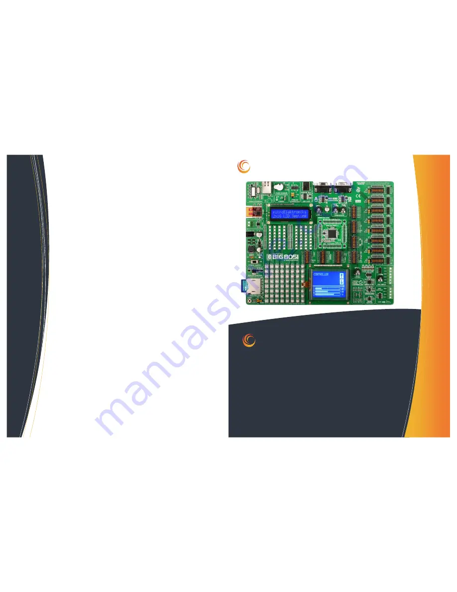
BIG 8051 Manual


1


User Manual 


Prepared By: 


Sajid Amir 
 
Computer Engineering‘15 
Elizabethtown College 


Josiah Buxton 
 
Computer Engineering ‘15 
Elizabethtown College 


BIG 8051 


Added resources from the works of: James Kelly and David Cain, 
Computer Engineering Elizabethtown College


Содержание BIG 8051

Страница 1: ...red By Sajid Amir Computer Engineering 15 Elizabethtown College Josiah Buxton Computer Engineering 15 Elizabethtown College BIG 8051 Added resources from the works of James Kelly and David Cain Computer Engineering Elizabethtown College ...

Страница 2: ...zo buzzer 9 8 DS 1820 temperature sensor 10 9 USB UART module 11 10 RS 232 modules 12 11 CAN module 13 12 ZigBee module 14 13 MMC SD connector 15 14 Comparator 16 15 ADC module 17 16 DAC module 18 17 Memory modules 19 18 LEDs 20 19 Push buttons 21 20 I O ports 22 21 8051 Assembly introduction 23 22 Register addressing 24 23 Instruction set summary 25 24 Instruction by opcode 27 25 Disclaimer 28 Pa...

Страница 3: ... Product CD USB Cable 128x64 graphic LCD display 2x16 alphanumeric LCD display Piezo buzzer CAN ZigBee System Specification Power Supply over AC DC connector USB Cable 5V DC Power Consumption 50mA with all modules off Dimensions 26 5 x 22 cm Weight 420g Features Full featured development system for 8051 Analog to digital conversion of voltage signal CAN communication module Back of BIG8051 develop...

Страница 4: ...rn on pull up pull down resistors 12 I O ports 13 A D converter inputs 14 D A converter outputs 15 Memory modules 16 Touch panel controller 17 Connector for GLCD display 18 Connector for touch panel 19 Push buttons 20 Jumper used to shorten protective resistor 21 Jumper used to select push buttons logic state 22 Reset button 23 Connector for MMC SD cards 24 3 3 V voltage regulator 25 Power supply ...

Страница 5: ...C connector CN18 Before you turn the system on it is necessary to place jumper J11 in the EXT position Next set the switch marked POWER SUPPLY to the ON position As soon as the development system now powers on a green LED labelled POWER will automatically illuminate Power Supply connector Power supply module connections schematic ...

Страница 6: ...040 Pinout 3 MCS 51 BIG8051 4K bytes internal ROM 128 bytes internal RAM Four 8 bit I O ports Two 16 bit timers Serial interface 64K external code memory space 64K external data memory space 210 bit addressable locations Pipelined instruction architecture executes 70 of instruction set in 1 or 2 system clocks Up to 25 MIPS throughout with 25MHz clock 4352 bytes internal RAM 64kB Flash in system pr...

Страница 7: ...g a USB DEBUG ADAPTER which is provided with the box It is always a good practice to make sure that the power is turned on the USB DEBUG ADAPTER is connected to the development system through the cable as shown CN23 JTAG programmer USB DEBUG ADAPTER Connector for programmer Connecting JTAG Programmer ...

Страница 8: ... Ethernet module lets us access the LAN network via the connector RJ45 Using Serial Peripheral Interface this module can communicate with the microcontroller Ethernet module Ethernet module connection schematic 4 Connecting Ethernet cable ...

Страница 9: ...his buzzer gives the BIG8051 development system the ability to emit audio signals Best performance for our Piezo buzzer can be achieved with frequencies between 2KHz and 4KHz To make a connection between the piezo buzzer and the microcontroller it is necessary to set switch 8 on the DIP switch SW13 to the ON posi tion The figure currently shows it in off position Piezo buzzer connected to the micr...

Страница 10: ... with 9 bit resolution and takes a maximum of 750ms The communication between this module and the microcontroller is achieved via pin P2 7 as shown in the diagram To establish a connection between them it is necessary to set switch 8 on the DIP switch SW15 to the ON position DS1820 and microcontroller connection schematic 6 DS1820 temperature sensor connected Make sure that the rounded side of the...

Страница 11: ...ler and the USB UART module it is important to set switches 1 and 3 optionally 2 and 4 to the ON position The BIG8051 can also use this module to power itself To achieve this it is necessary to set the switch position of jumper J11 found on the power module from EXT to USB SW13 Connecting USB cable USB connector and microcontroller connection schematic 7 USB UART module ...

Страница 12: ...m to communicate to external devices in compliance with the RS 232 standard The two RS modules in the BIG8051 can operate separately To connect switches 1 and 3 optionally 2 and 4 on DIP switch SW11 should be set to the ON position RS 232 module RS 232 module connection schematic 8 ...

Страница 13: ...Each CAN node is able to send and receive messages but not simultaneously The devices that are usually connected by a CAN network are typically sensors ac tuators and other control devices The host processor decides what the received messages mean and what messages it wants to transmit Sensors actuators and control devices can be connected to the host processor CAN controller stores the receives s...

Страница 14: ...for function ality At the moment our boards do not have any RF module attached to it However the MRF24J40MA ZigBee module can be connected to the development system This module can be used as an ideal solution for wireless sensor networks home automation building automation and consumer applications The features of this particular radio transceiver module are 2 4 GHz IEEE 8 2 15 4 Transceiver modu...

Страница 15: ...cards due to the on board MMC SD connector The module uses microcontroller pins for serial com munication To connect this module it is necessary to set switches 1 3 and 5 optionally 2 4 and 6 on the DIP switch SW10 as well as switches 1 and 2 on the DIP switch SW14 to the ON position ...

Страница 16: ...The BIG8051 can compare voltage levels due to a comparator built into the microcontroller Voltage signals are supplied via potentiometers P5 and P6 To enable voltage signals set switches 5 and 6 on DIP switch SW15 to the ON position ...

Страница 17: ...e 12 bit digital value The analog voltage signal is supplied via screw terminals CH0 CH1 CH2 and CH3 The ADC module is built in into the microcontroller The voltage supplied from the VREF pin is used as a voltage reference In order to use this voltage switch 8 on the DIP SW14 should be set to the ON position ...

Страница 18: ...ital values into appropriate analog voltage values The output analog voltage signals is delivered via screw terminals DAC0 and DAC1 Like the ADC module this module also uses the VREF pin on the microcontroller as a voltage reference To use this voltage switch 7 on DIP switch SW14 should be set to the ON posi tion ...

Страница 19: ... and 6 on the DIP switch SW10 as well as switch 7 on the DIP switch SW15 to the ON position The RAM module enables the microcon troller to use an additional 64Kbit RAM memory via SPI To enable this connec tion between the module and the micro controller it is necessary to set switches 1 3 5 7 and 8 optionally 2 4 6 on the DIP switch SW10 to the ON position EEPROM module enables the microcon trolle...

Страница 20: ... to visually indicate the state of each microcontroller I O pin When active an LED indicates that a logic 1 is present on that particular pin To enable LEDs to illuminate it is necessary to select the appropriate port using DIP switch SW9 There are 8 available ports labelled PORT0 through PORT7 ...

Страница 21: ...d to change the logic state of all the microcontroller input pins Jumper J10 is used to determine the logic state to be supplied on the appropriate microcontroller pin by pressing a push button On the lower left side of the push buttons a RESET button can be found to reset the micro controller ...

Страница 22: ...mpers J1 J8 to control this aspect The pull up resistor ensures that the signal will be a valid logic level if external devices are connected A pull up resistor weakly pulls the voltage of the wire it is connected to towards its voltage source level when the other components on the line are inactive A pull down resistor works the same way but is con nected to ground It holds the logic signal near ...

Страница 23: ...can conclude that the bit addressable memory located from 0x20 through 0x2F which provides 128 bits of bit addressable memory The upper portion is used general purpose RAM ad can be accessed by any addressing mode direct or indirect Special function registers SFRs have been added to the C8051 to that of the standard 8051 for enhanced peripherals Upper data memory and SFR memory share the same addr...

Страница 24: ... symbolizes that it is a hexadecimal number Similarly if we write a binary number it should end with B The 0 in the third instruction in 0FFH symbolizes that the F is a hex number and not a letter This is always necessary if we are writing any hex numbers It should always start with a 0 All the register should be assumed to be of 1 byte unless otherwise mentioned Now to transfer contents of R1 to ...

Страница 25: ...BIG 8051 Manual 25 Instruction Set Sum ...

Страница 26: ...BIG 8051 Manual 26 Instruction Set Summary cont ...

Страница 27: ...BIG 8051 Manual 27 Instructions by opcode ...

Страница 28: ...he recommended assembler is Keil uVision5 http www keil com c51 After both the installers are downloaded install the software and run the IDE first Then proceed to write your program in assembly language Assembling your Code Next you may be prompted to find an assembler Browse for the assembler Keil uVi sion 5 installed earlier Click rebuild all as shown After completing your code click the assemb...

Страница 29: ... the development board and the IDE power on the system as instructed earlier The jumpers J13 and J14 should be in the JTAG posi tion Click options and then select Connection Options from the drop down In the Collection Options Dialog Box select configuration as shown Click Connect to establish connection ...

Страница 30: ...BIG 8051 Manual 30 Downloading and Running Code on 8051 Click Download after connection has been established successfully Then click the Go button as shown Observe results on board ...

Страница 31: ...ening the simulator In the black box on the right you ll find a reference for how to access vari ous hardware elements of the simulated 8051 such as switches and LEDs and whether currently sees a logic 1 or 0 Make sure you have Java installed you can download it at http java com en download index jsp Run the installer you downloaded and make sure to uncheck installing the Ask Toolbar Download http...

Страница 32: ...un will run the program all the way to the end without stopping At any point the user may pause the program by clicking the button again 3 If you wish to stop the program from running entirely select RST This will end the program and allow you to make modifications or simply begin the program again 4 When finished you can save your code as a asm by clicking save which will allow you to import your...

Страница 33: ...BIG 8051 Manual 33 Simulation Video Amir Buxton https youtu be x5dIODI726U ...

Страница 34: ...s been executed before return to main SETB P0 0 set as flag that this function has been executed JMP aerate jump if this is the first time the switch read as pressed Switch2 JB P0 1 main If this function has been executed before return to main SETB P0 1 set as flag that this function has been executed JMP aerate jump if this is the first time the switch read as pressed Switch3 JB P0 2 main If this...

Страница 35: ... taken by Sajid Amir and should not be copied References http www mikroe com downloads get 1460 big8051_manual_v100 pdf http www silabs com Support 20Documents Software 8051_Instruction_Set pdf http www botskool com tutorials electronics 8051 introduction 8051 assembly language programming page 1 http users etown edu w wunderjt Xilinx 20instructions pdf http users etown edu w wunderjt Instructions...

Отзывы: