PolarFire FPGA 1G Ethernet Loopback Using IOD CDR
Microsemi Proprietary DG0799 Demo Guide Revision 3.0
6
2.3.3
IP Configuration
This section describes the IP blocks and user-defined blocks instantiated in the demo design.
2.3.3.1
PF_IOD_CDR_C0_0
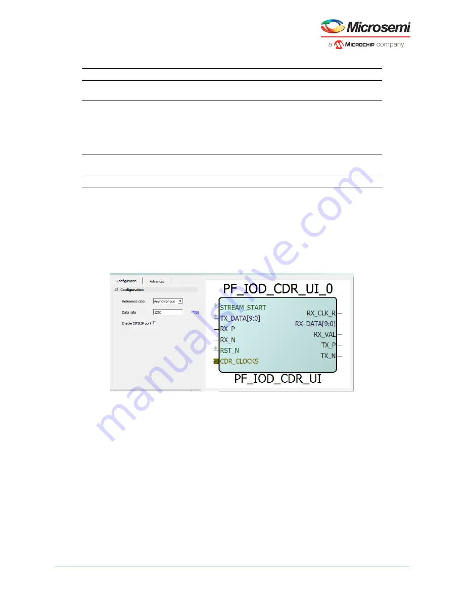
The PF_IOD_CDR_C0_0 (PF_IOD_CDR) block is configured for 1250 Mbps. The data rate is set to
1250 Mbps because the SGMII interface operates at this speed. The
Enable BITSLIP port
check box
is
not selected because the CoreTSE IP has a built-in word alignment logic.
Figure 3 •
PF_IOD_CDR Configurator
The Advanced tab includes the Jump step size option that specifies the precision of the clock adjustment
during clock recovery. The supported step sizes are 2 or 3, this demo uses a step size of 3.
page 6 shows the configuration of the PF_IOD_CDR_C0 block.
2.3.3.2
CORETSE_0
The CORETSE_0 (CoreTSE) block is used to implement the Ethernet MAC. This block is configured in
the ten-bit interface (TBI) mode to interface with the VSC PHY using the SGMII interface, as shown in
page 7. The
MDIO PHY Address
value is used by the Mi-V soft processor to read and write to
the Management registers of the CoreTSE IP. The Include receive slip logic option is not selected
because the CoreTSE IP has a built-in word alignment logic in TBI mode.
REF_CLK_SEL
Output
Reference clock speed pin of the VSC PHY. Held high for
selecting the 125 MHz reference clock speed.
RD_BC_ERROR
Output
CoreTSE receive error signal. This LED signal indicates the
receive code group error. This signal is synchronous to
RX_CLK_R and mapped to LED4 on the board.
When the LED is ON, there is an error in the received code
group.
When the LED is OFF, there is no error.
SPISCLKO, SPISS,
SPISDO, SPISDI
Output
SPI controller signals to interface with the ZL30364 clock
generation hardware.
TDO
Output
JTAG test data output. Serial data output to tap.
Table 2 •
I/O Signals
(continued)
Signal
Direction
Description


