


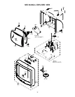


A
B
C
D
E
F
G
H
A
B
C
D
E
F
G
H
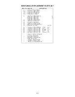
2
1
3
4
5
6
7
8
2
1
3
4
5
6
7
8
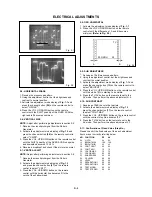
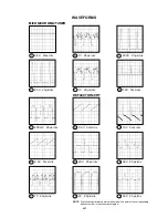
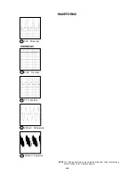
WAS RECEIVED IN GOOD CONDITION AND PICTURE IS NORMAL.
WITH THE DIGITAL TESTER WHEN THE COLOR BROADCAST
NOTE:THE DC VOLTAGE AT EACH PART WAS MEASURED
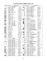
C607
1
F
C608
1
F
C616
1 F
C615
1 F
C609_1
0.01
B
C104
0.01
B
C611
1F
C629_1
0.01
B
C007_1
0.022
B
C627_1
0.01
B
C626_1
0.01
B
C624
1T
F
C101
0.01
B
C620
0.01 B
C639
0.01
F
C004
0.022
F
C113
560P
B
C102
0.01 B
C105
470P
B
C107
220P
B
C603
22P
CH
C001
0.01 F
C622
1
F
C605
1F
C641
0.001
B
C108
0.001
B
C602
0.1
F
C604_1
0.022
B
C610_1
47
16V
YK
C606_1
100
6.3V
YK
C103_1
470
6.3V
YK
C630_1
470
10V
YK
C632_1
470
10V
YK
C628_1
1
50V
KA
C118_1
470
6.3V
YK
C123_1
10
50V
YK
C623_1
2.2
50V
KA
C633_1
10
50V
YK
C601_1
1
50V
KA
C617_1
100
10V
YK
C621_1
47
16V
YK
R112
2.2K 1/4W
R113
2.2K
1/4W
R601
8.2K
1/4W
R103
1K
R102
1K
R609
120K
R611
10K
1/4W
R002
15K 1/2W
R610
12K
R613
100
1/4W
R614
100
1/4W
R603
120 1/2W
R607
100 1/4W
R615
100
1/4W
R608
1K 1/4W
R616
1K
1/4W
R618
22K
R617
47K
1/4W
R620
1K
1/2W
R003
100
R004
100
R104
1M
R120
470
R127
1K
R107
100
R108
100
R106
4.7K
1/4W
R129
47K
R119
22K 1/4W
R621
220 1/4W
R109
10K 1/4W
R110
10K 1/4W
R605
220 1/2W
R116
2.2K 1/4W
R115
22K
R123
10K 1/4W
R125
47K
R627
10K
R604
100 1/4W
R128
560
R126
2.7K
R101
560
R602
100
R606
22K
R001
15K 1/2W
R143
10 1/4W
R130
10K 1/4W
R105
4.7K
1/4W
OF PRINTING AND SUBJECT TO CHANGE WITHOUT NOTICE
NOTE: THIS SCHEMATIC DIAGRAM IS THE LATEST AT THE TIME
DANS LA NOMENCLATURE DES PIECES
N’UTILISER QUE CELLS DECRITES
DANGEREUSES AN POINT DE VUE SECURITE
:LES PIECES REPAREES PAR UN
ETANT
ATTENTION
:SINCE THESE PARTS MARKED BY
CAUTION
DESCRIBED IN PARTS LIST ONLY
CRITICAL FOR SAFETY,USE ONES
ARE
W836
W816
W801
W805
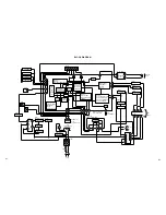
IC199
S-24C02BFJ-TB
MEMORY IC
1
2
3
4
5
6
7
8
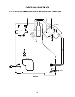
TUNER VIDEO SIGNAL
D602
MTZJ8.2B
D604
MTZJ8.2B
D001
MTZJ33B
DEFLECTION SIGNAL
B.SIGNAL
G.SIGNAL
R.SIGNAL
D606
1N4002-PAN
D603
1SS133
Q601
KTC3203_Y
5V REG
Q606
KTC3203_Y
8V REG
Q607
KTC3198
H.CTL
Q602
KTC3203_Y
5V REG
Q603
KTC3203_Y
5V REG
R629_1
22 3W
L101
3.3uH
0305
IC101
OEC7091B
MICON/CHROMA IC
1
10
11
12
13
14
15
16
17
18
19
2
20
21
22
23
24
25
26
27
28
29
3
30
31
32
33
34
35
36
37
38
39
4
40
41
42
43
44
45
46
47
48
49
5
50
51
52
53
54
55
56
57
58
59
6
60
61
62
63
64
65
66
67
68
69
7
70
71
72
73
74
75
76
77
78
79
8
80
9
SW104
EVQ21505R
VOL DOWN
SW103
EVQ21505R
VOL UP
SW102
EVQ21505R
CH DOWN
SW101
EVQ21505R
CH UP
SW105
EVQ21505R
POWER_ON
X601
100BT3R537
3.579545MHz
CP601
173979-6
1
2
3
4
5
6
L001
3.3uH 0305
TU001
ENG36A01GY
1
10
11
12
13
14
15
16
17
18
19
2
20
21
3
4
5
6
7
8
9
GND
B+
Vout
OS101
KSM-713SY
1
2
3
P.CON+5V
P.CON+5V
H_OUT
H_CTL
ABCL
B.OUT
CLAMP
H_CTL
G.OUT
R.OUT
H_SYNC
V_OUT
GND
V_FEEDBACK
AT+5V
ABCL
H_OUT
P.CON+5V
X-RAY
SDA
R.OUT
G.OUT
SCL
B.OUT
H_SYNC
AFT
UNREG+12V
KEY1
V_OUT
POWER_FAIL
KEY2
V_FEEDBACK
UNREG+12V
POWER_ON
GND
+B
REMOCON
AUDIO_OUT
AUDIO_MUTE
AUDIO_MUTE
VIDEO_IN2
AUDIO_IN2
X-RAY
AUDIO_OUT
P.CON+5V
IIC_OFF
P.CON+5V
TUNER+5V
GND
POWER_FAIL
AUDIO_IN2
VIDEO_IN2
TUNER+5V
AT+5V
TU_VIDEO
TU_AUDIO
SCL
AT+5V
SDA
KEY1
KEY2
REMOCON
POWER_ON
AFT
IIC_OFF
TU_AUDIO
SDA
SCL
+B
TU_VIDEO
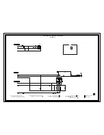
FROM/TO SOUND/AV
FROM TV POWER
G-2
G-1
TMD604
PCB010
NC
NC
NC
NC
NC
NC
NC
4.8
0
0
0
0
4.9
0
4.8
4.9
7.2
4.9
6 MCU VCC
7 TEST0
8 FILT
9 HLT
5 VSS
1 CNVSS
2 XIN
3 XOUT
4 TEST1
11 CVIN
10 VHOLD
12 RESET IN
13 MCU RESET OUT
14 Y SW OUT
15 V/C GND
16 3.58 XTAL
17 C-APC
18 MCU5.7V REG OUT
19 NC
20 CVBS IN3
21 AUDIO IN3
22 V/C VCC
23 MCU TEST
24 CVBS IN2
25 AUDIO IN2
26 CVBS IN1
27 AUDIO IN1
28 5.7V REG OUT
29 C(Y/C) IN
33 MONITOR OUT
32 FSC OUT
31 VREG VCC
30 Y(Y/C) IN
34 AUDIO ATT OUT
37 V RAMP F/B
38 V RAMP OUT
39 V RAMP CAP
40 8.7V REG OUT
Ver SYNC SEP
Ver.COUNT DOWN
V RAMP
Ver.Proc.
Hor.Proc.
SYNC SEPA/Hor.VCO
Hor.COUNT DOWN
AFC-1/H COINCIDENT
AFC-2 H PHASE
PGB OUTPUT Stage
DRIVE
CUT-OFF
HV BLK
IIC BUS
DECODER
OSD
ROM
RAM
CCD
CPU core
VCO
XO
COLOR CONT
RGB MATRIX
RGB Proc.1
RGB Proc.2
OSD SW
CONTRAST
BRIGHTNESS
MCU RESET
Power Manage.
MCU
CLK
Y MUTE
BLACK STRETCH
Vldeo Proc.
C-TRAP/YDELAY
SHARPNESS
Chroma Proc.
ACC/C-BPF
APC/KILLER
TINT/DEMO
ATT
VCXO
LPF
6bB AMP
MCU GND
IIC
TIM
AD
PWM
INT
I/O
CLK CONT
P-ON CONT
SDA/SCL
NC
NC
4.8
SCL
SDA
IIC_OFF
GND
NC
NC
35 AUDIO ATT FILTER
41 NC
42 HVCO F/B
43 AFC FILTER
44 DEF GND
45 FBP IN
46 H OUT
47 DEF VCC
48 NC
49 HI VCC
50 R OUT
51 G OUT
52 B OUT
53 ACL
54 NC
55 PROTECT
56 SDA
57 H_CTL
58 SCL
62 DEGAUSS_H
63 STANDBY_H
64 VOLUME
66 AFT
67 KEY1
68 KEY2
71 AV2
72 AV1
73 AUDIO_MUTE
77 SYNC
78 POWER FAIL
80 EXT_MUTE
76 ON_TIMER
60 NC
61 NC
75 IIC_OFF
65 NC
59 NC
70 REMOCON
69 POWER_ON
74 X-RAY
36
NC
NC
NC
4.8
2.4
4.9
4.9
4.9
4.8
0
4.9
4.9
2.8
4.8
0
0
4.8
0
4.9
NC
0
1.9
2.2
5.5
2.2
1.9
8.7
2.8
0.7
3.2
3.5
0
2.6
3.6
4.7
8.6
0
3.7
3.4
0
1.0
2.0
8.0
4.8
0
0
8.0
2.3
2.2
2.3
0.7
0
0
0
4.9
4.9
4.9
0
1.0
1.9
0.3
2.7
4.9
4.9
2.7
0
3.3
2.8
5.5
0
2.5
2.2
4.9
0
NC
6
5
7
3
2
4
1
5.5
8.8
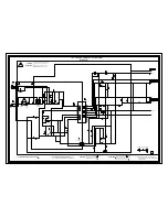
TEST POINT
FROM/TO DEFLECTION/CRT
6.0
5.0
5.6
NC
NC
NC
NC
NC
NC
NC
NC
NC
NC
NC
NC
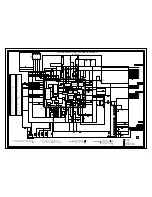
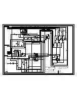
MICON/CHROMA/TUNER SCHEMATIC DIAGRAM
(MAIN PCB)
79 X-RAY_TEST
NC
1.9
11.3
7.9
8.5
0
0
0
0
0
0
4.8
0
4.8
5.5
7.2
5.5
4.9
VSS
E2
E1
E0
VCC
MODE
SCL
SDA
4.9
0
Содержание MT1194
Страница 30: ...M3R1 07Q O R NO SPEC NO W443056 ...