background image

Micro Crystal 


Low Power Clock Oscillator 32.768 kHz 


OV-7605-C8


June 2017 

20/20 

Rev. 1.0


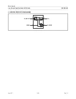
8.  COMPLIANCE INFORMATION 

Micro  Crystal  confirms  that  the  standard  product  Low  Power  Clock  Oscillator  OV-7605-C8  is  compliant 

with  “EU 

RoHS Directive” and “EU REACh Directives”. 
Please find the actual Certificate of Conformance for Environmental Regulations on our website: 

CoC_Environment_OV&OM-Series.pdf


9.  DOCUMENT REVISION HISTORY 

Date 

Revision # 

Revision Details 

June 2017 

1.0 

First release 


Information  furnished  is  believed  to  be  accurate  and  reliable.  However,  Micro  Crystal  assumes  no 
responsibility for the consequences


of use of such information nor for any infringement of patents or other 

rights  of  third  parties  which  may  result  from  its  use

In  accordance  with  our  policy  of  continuous 

development and improvement, Micro Crystal reserves the right to modify specifications mentioned in this 
publication without prior notice. This product is not authorized for use as critical


component in life support 

devices or systems. 


Micro Crystal AG 
Muehlestrasse 14 
CH-2540 Grenchen 
Switzerland


Phone  +41 32 655 82 82 
Fax     +41 32 655 82 83 
[email protected] 
www.microcrystal.com


Содержание OV-7605-C8

Страница 1: ...OV 7605 C8 Application Manual June 2017 1 20 Rev 1 0 Application Manual OV 7605 C8 Low Power Clock Oscillator 32 768 kHz...

Страница 2: ...ENCY VS TEMPERATURE CHARACTERISTICS 9 3 5 1 4 PACKAGE 10 DIMENSIONS AND SOLDER PAD LAYOUT 10 4 1 RECOMMENDED THERMAL RELIEF 10 4 1 1 MARKING AND PIN 1 INDEX 11 4 2 5 MATERIAL COMPOSITION DECLARATION E...

Страница 3: ...frequency output on CLKOUT pin can be enabled disabled by the CLKOE pin The CLKOUT frequency is enabled when CLKOE pin is connected to VDD When the CLKOE pin is tied to GND the frequency is disabled a...

Страница 4: ...kHz OV 7605 C8 June 2017 4 20 Rev 1 0 ORDERING INFORMATION 1 3 Example OV 7605 C8 20 20ppm TA QC Code Operating temperature range TA Standard 40 to 85 C Code Qualification QC Standard Commercial Grad...

Страница 5: ...ck Output push pull controlled by CLKOE If CLKOE is HIGH VDD the CLKOUT pin drives the square wave of 32 768 kHz When CLKOE is tied to Ground the CLKOUT pin is high impedance Hi Z GND 2 Ground CLKOE 3...

Страница 6: ...Micro Crystal Low Power Clock Oscillator 32 768 kHz OV 7605 C8 June 2017 6 20 Rev 1 0 DEVICE PROTECTION DIAGRAM 2 3 GND VDD CLKOUT CLKOE 2 1 3 4...

Страница 7: ...DD slew rate 0 5 V ms IDD VDD Supply Current CLKOUT disabled 1 VDD 3 0 V TA 25 C 450 650 nA VDD 5 0 V TA 25 C 680 900 VDD 3 0 V TA 40 to 85 C 1300 VDD 5 0 V TA 40 to 85 C 1800 Input CLKOE VI Input vol...

Страница 8: ...AL CHARACTERISTICS 3 3 Supply current IDD vs Supply voltage VDD TA 25 C CLKOUT disabled 0 1 2 3 4 5 VDD V 700 500 300 0 I DD nA 100 400 600 6 200 800 TIMING WAVEFORMS 3 4 CLKOUT enable disable time 32...

Страница 9: ...500 ms CLKOUT CLKOUT duty cycle 40 60 Xtal Frequency Characteristics f f Frequency accuracy 10 20 ppm f V Frequency vs voltage characteristics 1 6 V VDD 5 5 V 3 ppm V f fTOPR Frequency vs temperature...

Страница 10: ...age dimensions bottom view Recommended solder pad layout 0 85 max 1 2 0 45 0 45 2 0 0 45 0 45 1 2 4 3 0 3 0 7 1 1 0 7 0 7 0 7 Tolerances unless otherwise specified 0 1mm Drawing OV 7605 C8_Pack drw_20...

Страница 11: ...kHz OV 7605 C8 June 2017 11 20 Rev 1 0 MARKING AND PIN 1 INDEX 4 2 Laser marking OV 7605 C8 Package top view Automotive QA and Commercial QC Medical QM M623A1 1 2 4 3 Production Date Code Pin 1 Index...

Страница 12: ...r Cr 7440 47 3 94 Au Au 7440 57 5 3 Housing Ceramic 3 24 100 Al2O3 1344 28 1 4 Lid Ceramic 1 95 98 5 Al2O3 1344 28 1 Ceramic Lid Ni plating 1 0 Ni Ni 7440 02 0 Nickel plating Au plating 0 5 Au Au 7440...

Страница 13: ...id Plating nd nd nd nd nd nd nd nd nd nd nd nd nd nd 5 Seal Solder Preform nd nd nd nd nd nd nd nd nd nd nd nd nd nd 6 Terminations Int ext terminals nd nd nd nd nd nd nd nd nd nd nd nd nd nd 7 Resona...

Страница 14: ...Number Comment mg Quartz Crystal 1 Resonator 0 22 3 68 SiO2 14808 60 7 Chromium 2 Electrodes 0 0003 0 005 Cr Cr 7440 47 3 Ceramic 3 4 Housing Lid 5 16 85 80 Al2O3 1344 28 1 Gold 2 4 5 6 7 9 Electrodes...

Страница 15: ...age Description SON 4 Small Outline Non leaded SON ceramic package with ceramic lid Parameter Directive Conditions Value Product weight total 6 01 mg Storage temperature Store as bare product 55 to 12...

Страница 16: ...ORMATION OPERATING OV 7605 C8 6 1 OV 7605 C8 MCU VDD GND GND CLKOUT 2 VDD VDD 10 nF 1 CLKOE GPIO 1 A 10 nF decoupling capacitor is recommended close to the device 2 If CLKOE is HIGH VDD the CLKOUT pin...

Страница 17: ...max Ramp down Temperature Profile Symbol Condition Unit Average ramp up rate Tsmax to TP 3 C second max C s Ramp down Rate Tcool 6 C second max C s Time 25 C to Peak Temperature Tto peak 8 minutes max...

Страница 18: ...e PCB that have a fundamental or harmonic frequency close to 32 768 kHz This might cause breakage of crystal blanks due to resonance Router speed should be adjusted to avoid resonant vibration Ultraso...

Страница 19: ...and Trailer Minimum length 300 mm 4 0 1 2 23 0 05 1 43 0 05 2 0 05 4 0 1 1 0 0 2 5 1 5 0 1 3 5 0 05 1 75 0 1 8 0 3 0 254 0 02 0 83 0 05 0 1 0 061 Cover Tape 0 315 0 05 All dimensions are in mm OV 7605...

Страница 20: ...rmation furnished is believed to be accurate and reliable However Micro Crystal assumes no responsibility for the consequences of use of such information nor for any infringement of patents or other r...

Отзывы: