


Evaluates: MAX5863/MAX5864/MAX5865
MAX5865 Evaluation Kit
6
_______________________________________________________________________________________
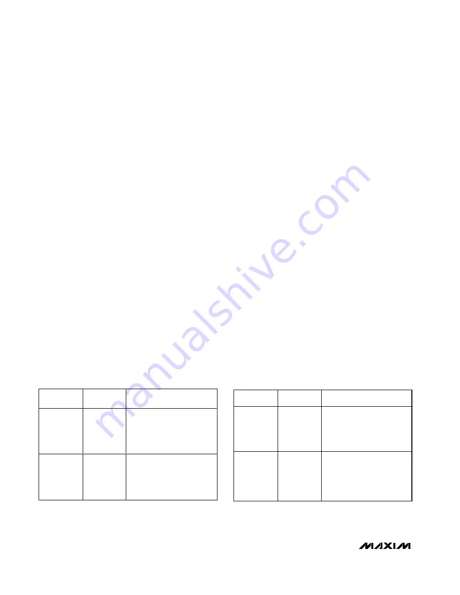
JU5
POSITION
JU6
POSITION
EV KIT FUNCTION
1-2
1-2
ID channel DC-coupled
differential output available at
the IDP (DAC voltage output)
and IDN (complementary DAC
voltage output) PC pads
2-3
2-3
ID channel differential output
converted to single-ended
signal using operational-
amplifier configuration;
available at ID SMA connector
JU7
POSITION
JU8
POSITION
EV KIT FUNCTION
1-2
1-2
QD channel DC-coupled
differential output available at
the QDP (DAC voltage output)
and QDN (complementary
DAC voltage output) PC pads
2-3
2-3
QD channel differential output
converted to single-ended
signal using operational-
amplifier configuration;
available at QD SMA
connector
Table 2. DAC ID Channel Analog Output
Selection
Table 3. DAC QD Channel Analog Output
Selection
Clock Signal
An on-board clock-shaping circuit generates a clock
signal from an AC sine wave signal applied to the
CLOCK SMA connector. The input clock signal should
not exceed a magnitude of 2.6V
P-P
. The frequency of the
signal determines the sampling frequency (f
CLK
) of the
MAX5865 EV kit circuit and should not exceed 40MHz.
The differential line receiver (U2) processes the input
signal to generate the CMOS clock signal. The clock sig-
nal’s duty cycle can be adjusted with potentiometer R13.
A 50% duty cycle is recommended. The clock signal is
available at the J1-2 header pin (CLK) and can be used
as the external clock for the logic analyzer.
Transmit Dual 10-Bit DAC Input
The MAX5865 integrates a dual 10-bit DAC capable of
operating with clock speeds up to 40Msps. The digital
data for the I and Q channels are alternately clocked
onto the DAC’s bus DD0–DD9. Data for the I channel is
latched on the falling edge of the clock signal and data
for the Q channel is latched on the rising edge of the
clock signal. The MAX5865 EV kit provides a 0.1in 2 x
10 header (J3) to interface a 10-bit CMOS pattern gen-
erator to the EV kit. The header data pins are labeled
on the board with the appropriate data bits designation.
Use the labels on the EV kit to match the data bits from
the pattern generator to the corresponding data pins on
header J3. Header pins J3-1 through J3-19 (odd pins)
are data pins DD0–DD9. All other header pins are con-
nected to digital ground OGND.
Transmit Dual DAC Outputs
The MAX5865 transmit DAC outputs are ±400mV
P-P
full-
scale differential analog signals and are biased to
1.4VDC common mode. The full-scale output and DC
common-mode level are set by the internal voltage refer-
ence. A variation in the reference voltage results in pro-
portional changes to the DAC full-scale output and the
DC common-mode level. The ID and QD outputs are
simultaneously updated on the rising edge of the clock
signal. The differential ID and QD output signals can be
sampled at the IDP, IDN, QDP, and QDN PC pads or
converted to single-ended signals using on-board opera-
tional-amplifier circuits. Configure jumpers JU5, JU6,
JU7, and JU8 to select the output signal format. See
Tables 2 and 3 to configure jumpers JU5–JU8. When
jumpers JU5–JU8 are configured for operational-amplifier
conversion, the differential signals are converted into a
50
Ω
single-ended signal with operational amplifiers U3
and U4. The single-ended output signals can be sam-
pled at the ID SMA connector for the ID channel and QD
SMA connector for the QD channel. When jumpers
JU5–JU8 are configured for DC-coupled differential out-
puts, the DC-coupled differential signals can be sampled
at the IDP and IDN PC pads for the ID channel. The QD
channel can be probed at the QDP and QDN PC pads.