background image

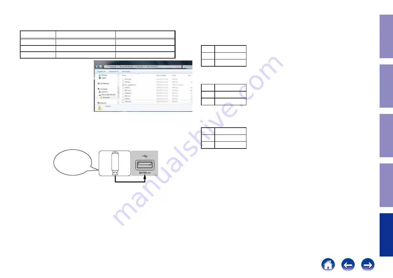
2.3. File structure on USB Memory

Copy the update files to the USB memory with the following structure.

USB memory root

Model Name

Model Area

Product ID

SR6011 U

North America (U)

100100500100

SR6011 N

Europe (N)

100100500200

SR6011 K

China (K)

100100500500

  + firmwares    

    + X00100XXXXXX

      + APLD.bin

      + VPLD.bin

      + DSP1.bin

      + DSP2.bin

      + DSP3.bin

      + DSP4.bin

      + enc_update.xml

      + GUI.bin

      + IMG.bcd

      + MAIN.bin

      + SBL.bcd

2.4. Insert the USB memory into the USB port.

NOTE : Remove the LAN cable from this unit when performing updates.

Download firmware 

in USB flash drive.

2.5. Start the update.

While holding down buttons "

TUNER PRESET CH +

" and "

STATUS

" simultaneously, press the power 

button to turn on the power.

2.6. Display during USB update

After around half minutes, display shows the following message.

L1

USB Updt

L2

 Start  

L3


2.7. Press the "ENTER" key on the remote control unit or this unit.

Then start Firmware Update.

L1

Update  

L2

File    

L3

Check   

2.8. The firmware update finishes.

When the update is completed, the following message appears on the display, then the unit returns to 

the normal status.

L1

Updating

L2

Complete

L3


---Cautions on Firmware Update---

• Never remove the USB memory before the update is finished.

•  Do not turn off the power until updating is completed.

• It takes around 1 hour to complete the update.

Once an update is started, normal operations cannot be performed until it is completed.

The GUI menu settings and image adjustment settings of this unit may be initialized.

Note down the settings before updating, and set them again after updating.

188

Caution in 

servicing

Electrical

Mechanical

Repair Information

Updating

Содержание SR6011

Страница 1: ... com SR6011 AP ZH index php CAUTION IN SERVICING ELECTRICAL MECHANICAL REPAIR INFORMATION UPDATING AV Surround Receiver SR6011 Service Manual Ver 4 For purposes of improvement specifications and design are subject to change without notice Please use this service manual with referring to the operating instructions without fail Some illustrations using in this service manual are slightly different f...

Страница 2: ...rts List Logging in to New SDI and Accessing the Parts List Accessing the Part List from the Model Asset Screen PRINTED CIRCUIT BOARDS Parts Table Downloading the Parts List as an Excel File Revision History Searching Part Numbers or Ref Numbers CAUTION IN SERVICING Initializing This Unit JIG FOR SERVICING 2 Caution in servicing Electrical Mechanical Repair Information Updating ...

Страница 3: ...chematic diagrams and parts lists be sure to use the designated parts Be sure to mount parts and arrange the wires as they were originally placed For safety seasons some parts use tapes tubes or other insulating materials and some parts are mount ed away from the surface of printed circuit boards Care is also taken with the positions of the wires by arranging them and using clamps to keep them awa...

Страница 4: ...A part ordered without specifying its part number can not be supplied 4 Part indicated by mark is not illustrated in the exploded view WARNING Parts indicated by the z mark have critical characteristics Use ONLY replacement parts recommended by the manufacturer Electrostatic breakdown of the semi conductors or optical pickup may occur due to a potential differ ence caused by electrostatic charge d...

Страница 5: ...h to change the CAPTCHA code and enter it again 4 Press the Login button 1 Access New SDI from the URL below http dmedia dmglobal com 2 When the login screen is displayed enter your username and password 3 Enter the 5 letters shown as the blue CAPTCHA code as single byte characters If the text is unclear click Refresh to change the CAPTCHA code and enter it again 4 Press the Login button 5 When th...

Страница 6: ... Screen PRINTED CIRCUIT BOARDS Parts Table 1 Display Model Asset from New SDI 2 Click the section displayed as Link to Part Lists under the model name NOTE If the Link to Parts List section is not displayed download the parts table from the Asset list 1 Display the Parts List Click the PCB name in the blue bar to display the parts list for the board Left and right arrow icons are displayed if the ...

Страница 7: ...and press the search button 2 The search results are displayed The name of the sheet in which the search part is used and the part s line are displayed 3 Next click the Sheet section of the search results 4 The Board Part Table opens and the line on which the searched part number appears is highlighted 7 Caution in servicing Electrical Mechanical Repair Information Updating ...

Страница 8: ...enter the service mode in step 3 repeat the procedure from step 1 Initializing the device restores the customized settings to the factory settings Write down your settings in advance and reconfigure the settings after initialization Use the following jigs extension cable kit when repairing the PCBs Order with your dealer for the jigs your dealer if necessary 8U 110084S EXTENSION UNIT KIT 1 Set 8U ...

Страница 9: ... DAC1 SCH30_MAIN DAC2 SCH31_SPK SCH32_REGULATOR SCH33_5CH AMP SCH34_4CH AMP SCH35_FRONT SCH36_HDAM1 SCH37_HDAM2 SCH38_SMPS PRINTED CIRCUIT BOARDS DIGITAL INPUT F HDMI CONNECT 2 CONNECT 3 CONNECT 4 VIDEO SIDE CNT GUIDE FRONT CONT FFC SPK SPK H2L GUIDE TRANS GUIDE TOP GUIDE SIDE 5CH AMP 4CH AMP FRONT HDMI FFC TOP FRONT CNT TUNER BKT HDAM SMPS LEVEL DIAGRAM FRONT ch CENTER SURROUND ch SUBWOOFER ch AS...

Страница 10: ...Z2 15 CJP15HJ282Z T203 21 20 19 18 17 16 15 13 14 12 11 9 10 8 7 5 6 4 3 1 2 22 23 24 25 26 27 BN24A CJP27HJ282Z C125Z2 27 2 1 3 4 6 5 7 8 10 9 11 12 14 13 15 BN26A CJP15HJ282Z C125Z2 15 T3 T4 T42 T62 T43 T242 T243 T244 T245 T48 T51 T317 T138 T148 T249 25 24 23 22 2 1 3 4 6 5 7 8 10 9 11 12 14 13 15 16 17 18 19 20 21 BN25A C125Z2 25 CJP25HJ282Z T128 R1007 OPEN R1008 0 T64 T65 T66 T67 T68 7 6 5 4 3...

Страница 11: ...3YTYH600 L1171 CB03YTYH600 L1172 OPEN L1173 OPEN L1174 CB03YTYH600 L1191 CB03YTYH600 L1192 OPEN L1193 OPEN L1194 CB03YTYH600 L1201 CB03YTYH600 L1202 OPEN L1203 OPEN L1204 CB03YTYH600 L1211 CB03YTYH600 L1212 OPEN L1213 OPEN L1214 CB03YTYH600 1 5 4 2 VIN VOUT EN GND OC 3 IC124 C1234 R1127 OPEN R1147 OPEN R1157 100 R1167 OPEN R1325 OPEN JIG PJ01 JIG PJ02 R1181 33 T173 C1190 OPEN C1408 0 1 50V C1181 0...

Страница 12: ...D4_CS DR_CK DR_CE DR_DIN DR_DOUT DA_MS DA_MC DA_MDI D5V_PW DA_PW DV_PW1 DV_PW2 CEC_PW CEC_PW2 R1552 0 MCU RC_IN RC_OUT_SR AV POWERKEY M_RESET BDOWN TU_RXMO SCL FL_CE FL_RST TU_INT FL_CLK FL_DATA RED_LED VSELA VSELB ISELA ISELB KEY1 KEY2 KEY3 REMOTEPOWER D5V_POWER CPUPOWER MAINPOWER THER_PROTA MVOLCLK1 MVOLDATA ZONE_CL ZONE_DA WHI GRN_LED FIL_CTRL M3 3V FL_CE2 FLASHER_IN_SR AV MAINPOWER M_RESET BDO...

Страница 13: ... 6 7 8 9 10 11 12 13 14 15 16 IC174 MC74HC4094ADR2G 1 2 3 4 5 6 7 8 9 10 11 12 13 14 15 16 IC175 MC74HC4094ADR2G C1704 0 1 C1705 0 1 1 2 3 4 5 6 7 8 9 10 11 12 13 14 15 16 IC176 MC74HC4094ADR2G C1706 0 1 R1701 4 7K 1 2 3 4 5 6 7 8 9 10 11 12 13 14 15 16 IC173 MC74HC4094ADR2G C1703 0 1 R1702 4 7K 1 2 3 4 5 6 7 8 9 10 11 12 13 14 15 16 IC177 MC74HC4094ADR2G C1707 0 1 M3 3V AEXP_OE AEXP_CLK AEXP_DATA...

Страница 14: ... C1906 0 01 R1929 33K C1907 0 01 T206 Q1906 ISA1530AC1 Q1907 2SC3052 Q1908 2SC3052 R1927 100 R1908 10K R1913 10K R1951 10K R1952 10K D1904 KDS160 D1903 KDS160 D1902 KDS160 D1901 KDS160 C1916 0 01 R1969 100 Q1922 2SC3052 R1967 3 3K R1966 10K R1968 3 9K 1 2 3 4 5 6 7 8 9 10 11 12 15 16 17 18 19 20 14 13 IC191 SN74LVC244APWR C1915 0 1 R1960 33 R1959 33 R1958 33 R1953 4 7K R1955 100 R1954 100 R1956 10...

Страница 15: ...0 1 2 3 4 5 6 7 8 9 10 11 12 13 14 15 16 17 18 19 20 21 22 23 24 25 26 27 28 29 30 31 32 33 34 35 36 37 38 39 40 41 42 43 44 45 46 47 48 IC202 PCM9211PTR R2053 680 C2015 10 6 3V C2018 10 6 3V C2017 0 1 R2048 4 7K R2050 47K C2022 OPEN R2051 1M X2001 24 576MHz R2032 4 7K R2044 100 C2023 50V 4700pF C2024 50V 0 068uF R2034 OPEN R2033 33 R2035 OPEN R2045 100 R2030 33 R2029 33 8 7 6 5 4 3 2 1 RN20133x4 ...

Страница 16: ...TA DIRLRCK DIRBCK DIRMCK DATAAD DACPCMF DACPCMCSW1 DACPCMS DACPCMSW2RSV DZF1 DIRPERR A 5V JTAG_TDOO JTAG_TDI JTAG_TMS JTAG_TCK APLD_CK APLD_DI APLD_CS RXMCK DSDMCK RXBCK DSDSCK RXLRCK DSD5 RXI2S0 DSD1 RXI2S1 DSD2 RXI2S2 DSD3 RXI2S3 DSD4 RXSPDIF DSD0 TXBCK TXLRCK TXI2S0 DA3 3V DA3 3V DA3 3V PLDAERR1 DIRNPCM DA3 3V DGND DEMZ3 DEMZ2 Z2DACBCK Z2DACDATA Z2DACLRCK Z2DACMCK Z3DACBCK Z3DACDATA Z3DACLRCK Z...

Страница 17: ...D_FLG0 TP42 TP43 TP44 R2553 33 R2556 33 R2555 33 R2552 33 R2551 OPEN R2543 33 C2528 1000P C2527 1000P C2526 1000P C2525 1000P C2524 1000P C2523 1000P C2522 1000P C2521 1000P C2520 1000P C2519 1000P C2518 1000P C2517 1000P C2516 1000P C2515 1000P C2514 1000P C2513 1000P C2512 1000P C2511 1000P C2510 1000P C2509 1000P C2548 1000P C2547 1000P C2546 1000P C2545 1000P C2544 1000P C2443 1000P C2542 1000...

Страница 18: ...2697 1000P C2696 1000P C2695 1000P C2694 1000P C2693 1000P C2692 1000P C2691 1000P C2690 1000P C2689 1000P C2688 1000P C2687 1000P C2686 1000P C2685 1000P C2684 1000P C2683 1000P C2682 1000P C2681 1000P C2680 1000P C2679 1000P R2645 4 7K C2645 1000P C2648 1000P C2650 1000P C2652 1000P C2653 1000P C2655 1000P C2657 1000P R2606 1M X2601 25MHz R2607 1 8K R2604 0 C2699 1000P R2638 33 1 2 3 4 5 6 7 8 9...

Страница 19: ...90 91 92 93 94 95 96 97 98 99 100 101 102 103 104 105 106 107 108 109 110 111 112 113 114 115 116 117 118 119 120 121 122 123 124 125 126 127 128 129 130 131 132 133 134 135 136 137 138 139 140 141 142 143 144 145 146 147 148 149 150 151 152 153 154 155 156 157 158 159 160 161 162 163 164 165 166 167 168 169 170 171 172 173 174 175 IC271 CVIADSP21487KSWZ 4B C2723 0 1 C2722 0 1 R2749 10K R2735 33 R...

Страница 20: ...92 93 94 95 96 97 98 99 100 101 102 103 104 105 106 107 108 109 110 111 112 113 114 115 116 117 118 119 120 121 122 123 124 125 126 127 128 129 130 131 132 133 134 135 136 137 138 139 140 141 142 143 144 145 146 147 148 149 150 151 152 153 154 155 156 157 158 159 160 161 162 163 164 165 166 167 168 169 170 171 172 173 174 175 IC281 CVIADSP21487KSWZ 4B C2833 0 1 C2832 0 1 R2849 10K R2835 33 R2813 1...

Страница 21: ...0K R3093 0 R3095 OPEN R3091 OPEN C3050 10 16V C3053 4700P R3090 100K R3094 0 R3096 OPEN R3092 OPEN R3087 33 R3088 1K C3054 1000P C3055 0 1 C3056 0 1 C3057 1000P C3058 1000P C3061 1000P C3062 1000P C3063 1000P C3064 1000P C3066 1000P C3067 1000P C3068 1000P C3069 1000P C3070 1000P C3071 1000P C3072 1000P C3073 1000P R3085 OPEN R3086 OPEN ADINL ADINR ADC ADCRST DGND A 5V A 5V DAGND DATAAD DIRADLRCK ...

Страница 22: ... 8 9 10 11 12 15 16 17 18 19 20 14 13 IC321 PCM5100PWR R3202 10K C3213 OPEN C3210 OPEN C3211 OPEN C3212 OPEN C3214 OPEN R3208 OPEN R3209 OPEN C3217 OPEN C3218 OPEN C3215 OPEN C3216 OPEN 1 2 3 4 5 6 7 8 9 10 11 12 15 16 17 18 19 20 14 13 IC322 OPEN R3207 OPEN R3201 10K R3206 OPEN R3205 10K R3210 OPEN 1 5 4 2 VIN VOUT STBY GND NC 3 IC323 BU33TD3WG R3211 10K ZONE_DAC A 5V DGND Z3DACMCK Z3DACLRCK Z3DA...

Страница 23: ...24 T225 T326 C5092 1 10V C5093 1 10V R5094 OPEN R5115 10 T20 C5116 OPEN C5117 OPEN T90 T91 R5093 10K C5095 OPEN C5101 0 1 R5091 0 R5092 OPEN C5111 0 022 1 2 3 4 5 6 7 8 9 IC502 MFI337S3959 1 2 3 4 5 6 7 8 IC503 BD82065FVJ E2 VBUSEN 1 2 3 4 5 6 7 8 9 10 JK501 KRJ 015XXNL CJJ9L029Z C5094 0 1 R5076 0 C5002 1000P C5011 4 7 6 3V C5012 4 7 6 3V C5013 0 1 C5014 0 1 C5021 4 7 6 3V C5022 4 7 6 3V C5023 0 1...

Страница 24: ..._150 T7 VDD_07 T8 GND_112 T9 GND_113 T10 GND_114 T11 GND_115 T12 GND_116 T13 GND_117 T14 GND_118 T15 GND_119 T16 GND_120 T17 GND_121 T20 AVDD_08 T21 AVDD_07 T22 AVDD_06 T23 AVDD_05 U1 TX_AVDD_03 U2 TX_AVDD_02 U3 GND_020 U4 TX_DDC_SCL U7 VDD_08 U8 VDD_09 U9 VDD_10 U10 VDD_11 U11 VDD_12 U12 VDD_13 U13 VDD_14 U14 TEST2 U15 GND_122 U16 GND_123 U17 GND_124 U20 AVIN13 U21 AVIN12 U22 AVIN11 U23 AVIN10 V1...

Страница 25: ...A_3CK_3 D3852 D3851 D3850 D3849 D3848 D3847 D3846 D3845 D3844 D3843 D3842 D3841 Q3861 RT1N141C Q3862 RT1N141C R3862 10K R3861 1K C3843 0 1 R3866 47K R3865 0 R3868 0 R3867 0 1 2 3 4 5 6 7 8 9 10 11 12 13 14 15 16 17 18 19 JK383 A0D7ABAR1990 HPD_3 R3874 47K R3873 47K 5V_4 T231 DA_4CK_4 D3872 D3871 D3870 D3869 D3868 D3867 D3866 D3865 D3864 D3863 D3862 D3861 Q3871 RT1N141C Q3872 RT1N141C R3872 10K R38...

Страница 26: ...981 2 2K R3982 8 2K 1 2 3 4 5 6 7 8 9 10 11 12 13 14 15 16 17 18 19 JK394 A0D7ABAR1990 D3974 OPEN D3973 OPEN D3972 OPEN D3971 OPEN D3970 OPEN D3969 OPEN D3968 OPEN D3967 OPEN D3966 OPEN D3965 OPEN D3964 OPEN R3979 0 R3978 10K CK_Z2 DA_Z2 5V_Z2 HPD_Z2 D3961 OPEN D3963 OPEN R3977 1 8K R3976 1 8K D3962 OPEN 1 2 3 4 5 6 7 8 9 10 11 12 13 14 15 16 17 18 19 JK391 A0D7ABAR1990 1 2 3 4 5 6 7 8 9 10 11 12 ...

Страница 27: ...043 0 1 C4046 0 1 C4047 0 1 C4048 0 1 C4049 0 1 C4050 0 1 C4051 0 1 C4052 0 1 C4053 0 1 C4054 0 1 C4055 0 1 C4056 0 1 C4057 0 1 C4045 0 1 C4044 0 1 C4058 0 1 C4059 0 1 R4088 open C4019 0 1 C4022 10 6 3V C4021 0 1 TP110 TP111 TP112 IP_RST TP114 TP115 TP116 TP117 TP118 TP119 R4057 OPEN R4058 OPEN R4071 2 7K 1 R4069 2 7K 1 R4083 open 1 2 3 4 5 6 7 CN401 10022H 07C CJP07GA193ZY R4050 0 R4051 0 R4052 0...

Страница 28: ...O8KI_Y0 G4 PO8KI_Y4 R0 PO8KI_C11 G3 PO8KI_C8 G0 PO8KI_Y8 R4 PO8KI_Y3 G7 PO8KI_Y5 R1 8KOPI_PCK PO8KI_VSYNC PO8KI_Y9 R5 PO8KI_Y6 R2 PO8KI_DE PO8KI_PCK PO8KI_Y7 R3 8KOPI_C3 B3 PO8KI_HSYNC PO8KI_Y11 R7 PO8KI_Y10 R6 8KOPI_C8 G0 8KOPI_C7 B7 8KOPI_C4 B4 8KOPI_C0 B0 8KOPI_Y0 G4 8KOPI_C11 G3 8KOPI_HSYNC 8KOPI_Y10 R6 8KOPI_Y3 G7 8KOPI_Y9 R5 8KOPI_Y11 R7 8KOPI_DE 8KOPI_VSYNC 8KOPI_Y6 R2 8KOPI_C2 B2 8KOPI_C5 ...

Страница 29: ...37 0 R4338 0 D4304 OPEN C4362 C4363 C4364 C4365 C4366 C4367 C4368 C4369 TP102 TP103 TP104 TP105 TP106 TP108 C4341 0 1 8 7 6 5 4 3 2 1 RN432 47x4 8 7 6 5 4 3 2 1 RN433 47x4 8 7 6 5 4 3 2 1 RN434 47x4 C4343 0 1 C4344 0 1 C4421 4 7 6 3V C4420 4 7 6 3V C4422 OPEN L4304 BLM21PG221SN1 TP107 1 2 3 4 5 6 7 8 9 10 11 12 13 14 15 16 17 18 19 JK432 OPEN 1 2 3 4 5 6 7 8 9 10 11 12 13 14 15 16 17 18 19 JK431 A...

Страница 30: ... NJU72750V C4601 0 1uF C4602 0 1uF 1 2 3 4 5 6 7 8 9 10 11 12 13 14 15 16 17 18 19 20 21 22 23 24 25 26 27 28 29 30 31 32 IC474 NJU72750V C4630 OPEN C4626 OPEN C4636 OPEN C4625 OPEN C4642 OPEN C4631 OPEN C4632 OPEN C4635 OPEN C4645 OPEN C4646 OPEN R4621 0 R4622 0 C4667 OPEN C4668 OPEN R4623 33 R4624 33 C4674 OPEN C4683 OPEN 1 2 3 4 5 6 7 8 9 10 11 12 13 14 15 16 17 18 19 20 21 22 23 24 25 26 27 28...

Страница 31: ...K Q8820 RT1P441C Q8813 RT1P441C Q8814 RT1N441C R8813 10K R8820 1K 2 1 3 4 6 5 7 8 10 9 11 12 14 13 15 16 17 18 19 20 21 BN26C C125Z2 21 1 2 3 4 5 6 7 8 9 10 11 12 13 14 15 16 IC898 MC74HC4094 C8991 0 1uF 1 2 3 4 5 6 7 8 9 10 11 12 13 14 15 16 17 18 19 20 21 22 23 24 25 CN88A C125Z1 25 C8777 22 50V R8781 220 R8779 100K C8779 330P R8777 100K R8773 220 Q8774 INC2001AC1 R8774 10K R8769 0 Q8770 INC2001...

Страница 32: ...18 19 20 21 22 23 24 25 26 27 CN87C C125Z1 27 1 2 3 4 5 6 7 8 9 10 11 12 13 14 15 16 17 18 19 20 21 CN89C C125Z1 21 1 2 3 4 5 6 7 8 9 10 11 12 13 14 15 16 17 18 19 20 21 22 23 24 25 CN88CC125Z1 25 21 20 19 18 17 16 15 13 14 12 11 9 10 8 7 5 6 4 3 1 2 22 23 24 25 BN88B C125Z2 25 21 20 19 18 17 16 15 13 14 12 11 9 10 8 7 5 6 4 3 1 2 22 23 24 25 26 27 BN87B C125Z2 27 21 20 19 18 17 16 15 13 14 12 11 ...

Страница 33: ...50V 1uF C5158 50V 1uF C5160 50V 1uF C5162 50V 1uF C5166 50V 0 1uF C5167 16V 100uF C5168 50V 0 1uF C5169 50V 0 1uF C5170 50V 0 1uF C5171 16V 100uF R5151 75 1 C5151 OPEN R5153 75 1 C5153 OPEN R5155 75 1 C5155 OPEN R5157 75 1 C5157 OPEN R5169 75 1 C5159 OPEN R5161 75 1 C5161 OPEN R5182 OPEN R5184 OPEN R5186 OPEN C5172 50V 68pF C5173 50V 68pF C5174 50V 68pF R5115 75 1 JK515 R5171 75 1 R5172 OPEN R5174...

Страница 34: ... Q5311 RT1P141C Q5313 RT1P141C Q5314 RT1P141C Q5312 RT1N141C Q5315 2SC3052 2 1 3 4 6 5 7 BN28B C125Z2 07 JK531 C5332 50V 0 1uF C5333 50V 0 01uF C5326 50V 0 1uF C5327 50V 0 01uF C5328 50V 0 1uF C5329 50V 0 01uF C5330 50V 0 1uF C5331 50V 0 01uF L5166 60R 3A BEAD L5165 60R 3A BEAD L5164 60R 3A BEAD L5311 60R 3A BEAD L5312 60R 3A BEAD L5313 60R 3A BEAD L5314 60R 3A BEAD L5315 60R 3A BEAD C5314 50V 0 1...

Страница 35: ...PEN C5259 OPEN R5258 100 C5254 OPEN C5255 OPEN C5256 50V 0 1uF R5255 100 OUT GND VS 1 2 3 RC521 HM336R R5259 OPEN D5258 OPEN Q5254 OPEN Q5253 RT1P441C 1 2 3 JK523 PJ 308 02 Q5212 RT1N141C 6 5 4 3 2 1 Q5211 FDC608PZ R5212 2 7K R5211 4 7K C5213 50V 0 1uF D5211 Z16V 0 5W C5212 50V 0 1uF R5210 0 C5215 50V 0 1uF R5213 10K C5211 50V 0 01uF 1 2 3 JK525 PJ 308 02 D5252 KDS160 C5251 50V 1000pF D5253 OPEN R...

Страница 36: ...5V B PIRIN_AVR TRIGGER_1 232I_MO 232O_MI REMOTE3 3V M3 3V DGND NC NC A 7V A 7V RTNGND RTNGND TRG 12V VIDEO 5V VIDEO 5V VGND TUNER_R TUNER_L TU_GND CN28C J9633 OPEN CN28B J9662 TU_ 5V TU_GND TU_CE TU_RST TU_INT TU_RXMO SCL TU_TXMI SDA TU_GND TU_ 5V TU_GND TUNER PART TP TP TP TP TP TP TP TP TP TP TP TP TP TP TP TP TP TU_ RST TU_INT TU_TXMI SDA TU_RXMO SCL TU_SEN DGND ZONE_DA ZONE_CL MVOLCLK1 MVOLDAT...

Страница 37: ...DA CE RST INT CHASSIS OPTION A CHASSIS L OUT R OUT VCC SCLK SDIO CE RST INT TUNER PART SCL SDA CE RST INT TUNER MODULE TU901 OPTION CNVYST990 D8E2 CNVYST990 A9U2 AREA N A EUR ANALOG TUNER OPEN JPN CHN CNVYST990 A2J1 TU_INT TU_RST TU_CE TU_TXMI SDA TU_RXMO SCL TU_GND TUNER_R TU_GND TUNER_L TU_ 5V TO CONNECT A PART PAEG 27_A4 FFC CABLE A B A OUTPUT A INPUT A INPUT V B INPUT B INPUT B OUTPUT V TU_GND...

Страница 38: ...R3002 1K C3003 0 1uF R3004 4 7K C3007 10V 1uF C3002 10V 1uF C3001 6 3V 10uF C3005 10V 1uF R3038 820 R3036 22K R3034 OPEN R3040 820 R3042 22K R3044 OPEN R3011 15K R3012 15K R3014 15K R3016 150K R3017 150K R3018 150K R3020 12K R3022 12K R3024 470 R3026 470 C3012 1800pF C3016 270pF C3017 270pF C3018 270pF R3031 15K R3029 15K R3033 150K R3035 12K R3037 470 R3039 470 R3041 12K R3043 150K R3030 15K R303...

Страница 39: ...12K R3115 150K R3116 150K R3118 12K R3119 470 R3120 470 R3121 470 R3123 12K R3125 150K R3126 150K R3124 12K R3122 470 C3121 1800pF C3122 1800pF C3123 270pF C3124 270pF C3125 270pF C3126 270pF R3145 100 R3147 100 C3138 OPEN C3137 OPEN R3131 15K R3129 15K R3130 15K R3132 15K R3135 12K R3133 150K R3134 150K R3136 12K R3137 470 R3138 470 R3139 470 R3141 12K R3143 150K R3144 150K R3142 12K R3140 470 C3...

Страница 40: ...RT1N237C D9230 KDS160 C9221 100 50V C9540 0 01uF M C9541 0 01uF M C9621 OPEN C9641 1000pF C9620 OPEN C9640 1000pF C9703 0 1u 250V JW922A J7 LAND J8 LAND 2 1 JK930 2 1 JK931 C9518 OPEN C9519 OPEN C9520 OPEN C9521 OPEN C9516 OPEN C9517 OPEN C9514 OPEN C9515 OPEN C9513 OPEN C9511 OPEN C9512 OPEN 2 1 JK922 2 1 JK921 2 1 JK923 2 1 JK925 2 1 JK924 2 1 JK927 2 1 JK926 2 1 JK929 2 1 JK928 R9208 1W 10 L920...

Страница 41: ...9332 OPEN R9333 OPEN R9334 OPEN R9335 OPEN D9339 1N4007 D9340 1N4007 C9334 0 1uF M D9335 OPEN D9336 1N4007 D9331 1N4007 D9332 OPEN D9333 1N4007 D9334 OPEN D9337 OPEN D9338 1N4007 C9333 0 1uF M C9332 0 1uF M C9331 0 1uF M D9343 1N4007 D9344 OPEN D9345 1N4007 D9346 OPEN D9347 OPEN D9348 1N4007 D9349 OPEN D9350 1N4007 C9337 0 1uF M C9336 0 1uF M C9335 0 1uF M D9306 OPEN C9306 10 50V D9307 OPEN R9306 ...

Страница 42: ...7315 OPEN ZD736 OPEN D7316 OPEN R7331 2W 0 47 R7333 2W 0 47 R7334 2W 0 47 R7332 2W 0 47 R7329 1W 22 C7329 OPEN R7330 1W 22 C7330 OPEN Q7332 2SB1647 Q7331 2SD2560 C7331 100V 10uF C7332 100V 10uF R7335 10K 1608 3 2 1 CN735 R7336 10K 1608 R7340 10K 1608 R7339 100K D7339 1SS133M R7338 PTC 115 C 470 ohm R7337 680K 1608 C7338 50V 0 1uF 1608 R7341 5 6K 1608 R7342 OPEN Q7338 MMBT5401 Q7339 MMBT5551 R7343 ...

Страница 43: ...22K R7745 22K R7801 1 2K R7802 470K C7801 50V 47uF RA3 C7802 100V 470pF J R7803 33K R7804 1K 3 C2 E B2 C1 B1 2 4 5 1 Q7804 HN4A06J C7804 100V 220pF C7808 OPEN Q7814 MMBT5401 C7807 2200pF M C7805 OPEN R7816 1 2K 1608 R7817 1 2K 1608 ZD784 Z5 1V R7815 OPEN R7807 0 1608 R7806 390 1608 R7805 1W 1K R7808 1W 1K C7803 OPEN R7814 27K 1 2W D7805 OPEN D7806 OPEN C7806 25V 220uF C7811 OPEN C7812 100V 220pF R...

Страница 44: ...6 OPEN R6129 OPEN R6001 10K 1 4 5 8 9 10 11 12 3 17 F TEST NC CLK INT CS RESET OSC 13 14 15 16 NC VDD DIO LGND 20 VH F 18 6 7 PGND NC NC NC FL601 GP1261AI C6091 1 50V C6012 0 1uF 1608 C6061 0 1uF C6062 0 1uF C6018 OPEN C6019 OPEN C6020 OPEN C6021 OPEN C6022 OPEN C6023 OPEN C6024 OPEN C6025 OPEN C6026 OPEN C6027 OPEN C6028 OPEN C6030 OPEN C6095 OPEN LUG61 Front Panel LUG63 OPEN LUG64 OPEN LUG65 CHA...

Страница 45: ...5 6K R8184 5 6K Q8186 KTC3875S Q8188 KTA1504S R8186 22 R8188 22 R8190 220 R8152 33K C8154 220P R8176 1M C8176 220P R8192 100 C8201 10 50V RA3 R8203 150 C8245 10 50V RA3 R8219 22 R8217 22 Q8221 KTA1504S Q8223 KTC3875S R8209 5 6K R8211 5 6K D8213 KDS160 R8213 470 D8215 KDS160 R8215 470 Q8227 KTA1504S Q8229 KTC3875S R8221 330 R8223 330 C8247 10 50V RA3 Q8213 KTC3875S Q8215 KTA1504S Q8205 KTA1504S Q82...

Страница 46: ... C8397 10 50V RA3 Q8363 KTC3875S Q8365 KTA1504S Q8355 KTA1504S Q8357 KTC3875S R8357 22 R8355 22 R8377 22 R8379 22 R8381 5 6K R8383 5 6K Q8385 KTC3875S Q8387 KTA1504S R8385 22 R8387 22 R8389 220 R8351 33K C8353 220P R8375 1M C8375 220P R8391 100 C8352 10 50V RA3 R8354 150 R8370 22 R8368 22 Q8372 KTA1504S Q8374 KTC3875S R8360 5 6K R8362 5 6K D8364 KDS160 R8364 470 D8366 KDS160 R8366 470 Q8378 KTA150...

Страница 47: ...XA562ES R9004 330K C9006 0 1uF 1608 C9007 OPEN C9008 0 1uF 1608 C9010 OPEN R9006 1M 1608 D9006 1N4007 D9005 1N4007 D9001 1N4007 D9002 1N4007 D9003 1N4007 D9004 1N4007 CX902 0 1uF 275VAC R9015 4 7K 1608 R9016 10K 1608 R9014 270K 1608 R9010 1M R9008 2 2M ZD908 120V 5W R9009 2 2M ZD911 150V 5W C9012 2200p DC1KV CX901 0 1uF 275VAC F9001 CY902 470p 250V CY901 470p 250V 2 1 CN902 C9001 0 01uF 250V R9017...

Страница 48: ...1 C1341 C1331 C1311 R3526 R3524 R3522 R3520 Q1117 Q1120 Q1119 R1561 R2671 R2571 IC111 IC116 IC115 IC114 IC112 R1133 R1213 R1203 R1193 R1173 R1183 R1125 R1165 R1145 R1144 R1114 R1164 R1154 R1124 L1115 L1165 L1145 L1125 L1155 C1115 C1114 C1116 C1126 C1166 C1164 C1165 C1124 C1156 C1154 C1155 C1146 C1144 C1145 C1125 C1113 C1112 C1123 C1122 C1163 C1162 C1153 C1152 C1143 C1142 Q1104 Q1103 R3525 R3523 R3...

Страница 49: ...FL 2 AGND 1 PRESW2 1 ZONE_DA 2 ZONE_CL 4 MVOLCLK1 3 ZONE_STB 5 MVOLDATA 6 VOL_MUTE 7 VAUXL 8 AGND 9 VAUXR 10 AGND 11 MIC 12 MICGND 13 DAZONE2L 14 DAGND 15 DAZONE2R 16 DGND 17 DAZONE3L 18 DGND 19 DAZONE3R 1 AGND 2 AGND 3 AGND 4 A 7V 5 A 7V 6 A 7V 8 AGND 7 A 7V 9 TUNER_L 10 AGND 11 TUNER_R 18 P_PREZ2MUTE 17 P_PREZ3MUTE 16 SEL_CLK 15 SEL_DATA 14 AEXP_Q S 12 AEXP_DATA 13 AEXP_STB 11 AEXP_CLK 10 AEXP_O...

Страница 50: ...Pb Pb JW97 JW96 JW98 CUP12857Z_A 2_MP JW99 2 14 15 1 11 10 2 1 7 6 1 11 10 4 13 2 1 7 6 2 1 11 10 20 21 25 24 2 10 11 1 18 19 2 14 15 1 11 10 2 1 11 10 1 12 2 13 2 14 15 1 11 10 J9611 J9616 J9615 J9606 J9601 J9608 J9613 J9605 J9627 J9603 J9617 J9612 J9621 J9622 J9623 J9624 J9625 J9604 J9626 CN27A CN961 CN64C CN27B CN23C CN23A CN28B BN77D J9631 CN28C CN27C JW961 J9633 J9662 J9661 J9632 CN9601 CN960...

Страница 51: ... JW932A JW933A JW934A JW923A JW923C JW935A CN711 CN712 IC936 F9338 F9337 F9336 R9917 R9916 IC937 D9233 D9234 D9303 D9304 D9331 D9332 D9333 D9334 D9335 D9336 D9337 D9338 D9339 D9340 D9342 D9343 D9344 D9345 D9346 D9347 D9348 D9349 D9350 D9355 D9356 J9342 C9317 C9318 J9215 J9216 JW955A JW955B D9701 C9324 C9710 C9222 C9223 C9224 C9225 C9226 C9227 C9228 C9229 C9230 C9231 C9232 C9233 C9234 C9235 C9236 C...

Страница 52: ...Q7238 Q7214 Q7138 Q7114 Q7001 D7519 D7516 D7515 D7506 D7505 D7419 D7416 D7415 D7406 D7405 D7319 D7316 D7315 D7306 D7305 D7219 D7216 D7215 D7206 D7205 D7119 D7116 D7115 D7106 D7105 R7116 R7117 R7416 R7317 R7316 R7217 R7216 C7238 C7138 C7518 C7511 C7505 C7418 C7411 C7405 C7318 C7311 C7305 C7218 C7211 C7205 C7118 C7111 C7105 C7408 C7308 C7208 C7108 C7538 C7438 C7338 C7523 C7423 C7323 C7223 C7123 C700...

Страница 53: ... C6060 C6059 C6230 C6229 C6228 C6227 C6226 C6104 C6103 C6102 C6101 C6098 C6095 C6076 C6070 C6069 C6022 C6061 C6052 C6051 C6039 C6030 C6028 C6027 C6026 C6025 C6024 C6023 C6062 C6021 C6020 C6019 C6018 C6015 C6013 C6012 C6011 C6009 C6004 C6003 C6002 C6001 C6067 C6066 C6065 C6054 C6053 C6044 C6042 C6038 C6037 C6036 C6035 C6008 C6007 C6006 C6033 C6078 C6014 R6118 R6086 R6100 R6099 R6092 R6019 R6108 R61...

Страница 54: ...1 13 DACDATA 12 DACCLK 11 DACMS 10 DA3 3V 9 DGND 8 ADINR 7 AGND 6 ADINL 5 AGND 4 A 5V 3 A 5V 24 DAC CSW1 26 DAC SW2 21 DACLRCK CN24A 22 A 5V 23 P_MUTE 3 0V 24 P_RL B 25 P_RLGND 21 A 5V 20 DGND 19 FANCONT_ON1 18 FANCONT_L_ON1 17 AMPSIGDET 16 Hi B_RLY 15 CURRENT_DET 14 SPRL_H2 10 DGND 13 SPRL_H1 12 SPRL_RSV4 11 DGND 9 SPRL_RSV1 8 SPRL_SB 7 SPRL_S 6 SPRL_C 5 SPRL_F 4 H P_RLY 3 H PR 2 H PGND 1 H PL Pb...

Страница 55: ... 319mVrms ACM2 DM A409 Sensitivity 38 8dB Pa 11 48mV Pa at94dBSPL Operation Voltage 5 0V 94dBSPL is expected to 11dBFS MIC IN 11 48mVrms 851mVrms 37 60dB 23 7dB 150mVrms 2 5dB LINE IN EXT IN NJU72750 NJU72751 8 5dB NJU72750 HDAM GAIN Setting of MASTER VOL 00dB B d 5 2 B d 5 0 B d 0 2 L A T I G I D S E Y W S SW YES ANALOG 2 0dB 0 5dB 3 0dB 0 5dB SW NONE DIGITAL 2 0dB 0 5dB 12 0dB 9 5dB SW NONE ANAL...

Страница 56: ...Basic OFFSET of VOL 0dB indication valude Fine tuning by software Digital input OFFSET of SW NONE OFFSET of A D input EXT IN SPEAKER OUT DSP x4pcs NJU72343 GAIN ADJ PRE OUT MUTE PCM1690 D A PLD PRE OUT 4 24Vrms 8Ω 2 5dB L P F GAIN 2 6dB 200mVrms Headroom 3dB Volume IC NJU72343 NON CLIP MAX SIGNAL LEVEL 4 2Vrms 0 5dB 150mVrms 2 5dB LINE IN EXT IN HDAM 2 83Vrms 0dBFS 10dBFS 20dBFS 30dBFS 40dBFS PCM1...

Страница 57: ...0dB DIGITAL IN 2 0dB 0 5dB 14dB 11 5dB ANALOG IN 2 0dB 0 5dB 14dB 3 0dB 14 5dB Basic OFFSET of VOL 0dB indication valude Fine tuning by software Digital input Voltage due to hardware of analog input Correction of Subwoofer OFFSET of A D input 11 5dB L P F GAIN 3 3dB 14 5dB 2 5dB LINE IN EXT IN 34dBFS DIG IN PCM 40dBFS DIG IN DD DD INPUT 30dBFS LFE 30Hz PCM INPUT 20dBFS L R 37dBFS A D IN ANA INPUT ...

Страница 58: ...B 0 5dB 3 0dB 0 5dB Basic OFFSET of VOL 0dB indication valude Fine tuning by software Digital input OFFSET of SW NONE OFFSET of A D input EXT IN SPEAKER OUT DSP x4pcs NJU72343 GAIN ADJ PRE OUT MUTE PCM1690 D A PLD PRE OUT 4 24Vrms 8Ω 2 5dB L P F GAIN 2 6dB 200mVrms Headroom 3dB Volume IC NJU72343 NON CLIP MAX SIGNAL LEVEL 4 2Vrms 0 5dB 150mVrms 2 5dB LINE IN EXT IN NJU72750 HDAM 2 83Vrms 0dBFS 10d...

Страница 59: ...OUT 4 24Vrms 8Ω 29dB MAX SIGNAL LEVEL 20dBFS DIG IN SPEAKER OUT 2 0Vrms 0dBFS 10dBFS 20dBFS 30dBFS 40dBFS PCM5100 2 5dB PRE OUT 150mVrms MONO HPF MONO NJW1194V Z2 PRE OUT MUTE NJW1194V MAX OUTPUT 4 2Vrms NJU72750 LINE NJU72750 To MAIN PCM5100 Z2 DAC 30dB 59 Caution in servicing Electrical Mechanical Repair Information Updating ...

Страница 60: ...one2 L Zone3 R Zone3 L PRE SW2 PRE ASS3R PRE ASS3L PRE ASS2R PRE ASS2L PRE ASS1R PRE ASS1L PRE SR PRE SL PRE SW1 PRE CEN PRE FR PRE FL Zone3 R Main L Main R ATT DIGITAL AUDIO BLOCK_C1 FL FR C SW SL SR SBL SBR 7 1ch EXT IN EXT_FL EXT_FR DAC DASW1 EXT_C EXT_SW DASL EXT_SL DASR EXT_SR EXT_SBL EXT_SBR DAASSIGN3R DAASSIGN3L DAASSIGN2R DAASSIGN2L DASW2 HDAM DAASSIGN1R DAASSIGN1L PRE ASS1R PRE ASS1L PRE ...

Страница 61: ...138 92 75 97 100 95 74 101 77 55 103 98 99 86 94 73 88 89 96 138 92 75 97 87 86 77 76 73 74 98 99 103 89 100 94 88 96 138 ADCRST DIRCE DIRDIN DIRDOUT DIRCLK DIRRST DSPMOSI 51 DSPMISO 52 DSPICLK 53 DSP_RST DSP_ICS DSP1FLAG0 From MAIN CPU To MAIN DIR From Z2 DIR 6 DEMPZ2 To Z2 DAC 10 34 26 24 23 25 6 13 DSP_RST DSP2_ICS DSP2FLAG0 DSP2FLAG3 DSP_RST DSP3_ICS DSP3FLAG0 From To MainCPU From To MainCPU F...

Страница 62: ...OUT PB COMPONENT OUT PR Blu Ray_V V_AUX_V VI1 VI2 VI3 VI4 VI5 SW1 VO2 CBL SAT_V 75 75 75 PROUT PBOUT YOUT 6dB 6dB 6dB CBL SAT_Y CBL SAT_PB CBL SAT_PR DVD_Y DVD_PB DVD_PR NJM2595MTE1 NJM2586AVC3 SW1 SW2 PS CH1 IN1 CH1 IN2 CH1 IN3 CH2 IN1 CH2 IN2 CH2 IN3 CH3 IN1 CH3 IN2 CH3 IN3 CH1 OUT CH2 OUT CH3 OUT DEC_Y_IN DEC_PB_IN DEC_PR_IN DEC_CVBS_IN 75 DVD_V VO1 SW2 SW3 SW4 SW5 HDMI BLOCK_B6 62 Caution in s...

Страница 63: ...VIDEO SIGNAL OUT VIDEO INPUT DIGITAL AUDIO BLOCK_B6 ANALOG HDMI Rx P1 TX Matrix SW 600MHz Rxlink0 Txlink0 Txlink1 4K 2K Up Scaler HDMI Tx Matrix SW 600MHz 600MHz DDR2 INTERFACE CONTROL Video Processor 1080P OSD IP Conv 4K 2K 4K 2K WITH TMDS EPM570F256C4N Z2HDMISPDIF RXI2S0 3 RXSPDIF HDMI SW1 MN864788 920PCK 920VD0 7 920PCK 920VD0 7 TXDATA0 TXBCK TXLRCK TXDATA0 TXBCK TXLRCK RXMCK RXBCK RXLRCK RXINT...

Страница 64: ...FLASH 4 PCM1690 2 TC74VHCU04 NJM2845DL118 DA1 8V 1 862A DA_POWER OPEN 0 04A IC113 IC114 IC115 IC116 IC117 IC119 IC120 IC121 Q1106 Q1104 FL5V Q1102 E POWER3 0 21A AD55 058Z 0 ADV8003 8B AD55 058Z 0 ADV8003 8B CS210010 CZZR APLD Q1101 E_POWER1 MN864788 2 MN864787 1 DA_POWER2 DIGITAL POWER Control terminal DA1 1V ON OFF S w i t c h e d H ON CPU_POWER MAIN CPU POWER Control terminal POWER ON H Case of...

Страница 65: ...7 24 BN63A CWB1C005100CC WIRE 5P 2mm 100mm UL1007 24 BN63B BN63B BN605 CWB8A005430HC WIRE 5P 2mm 430mm UL2725 24 28 1P 2C USB USB JACK FRONT VFD PCB CUP12866Z 1 CJP40GB284ZN CN69A FFC WAFER 40P 1mm CJP07GB03ZY WAFER 7P 2 5mm CN605 FRONT HDMI PCB FFC WAFER 23P 1mm CJP23GA333ZR CN101 CUP12860Z 5 PRI WIRE 2P 3 96mm 130mm WIRE 5P 3 96mm 220mm AMP PWR S1 S5 S6 WIRE 4P 2 5mm 270mm FL PWR WIRE 4P 2 5mm 2...

Страница 66: ...s pin should be High Not used it should be Low 11 PJ5 VSEL A I I I I Master Volume Rotary encoder signal input pin 12 VSS VSS Ground pin 13 PJ3 VSEL B I I I I Master volume Rotary encoder signal input pin 14 VCL VCL I Smoothing capacitor connection pin 15 VBATT VBATT Power supply pin 16 NC NC I Pd NC Pull down 17 TRST PF4 TRST NC NORMRAL I I Pd I I I I I I E20 Emulator control pin When normal oper...

Страница 67: ...IDEO I2C control pin for ADV8003 ADV7850 ADVM2000 except SR6011 79 P82 TXD10 DSP MOSI O DA3VPu L L L DSP ADI control pin 80 P81 RXD10 DSP MISO I DA3VPu L L L DSP ADI control pin 81 P80 SCK10 DSP CLK O DA3VPu L L L DSP ADI control pin 82 PC4 SCK5 DSP1FLAG0 DSP CS I Pd L L L DSP ADI interrupt signal input pin Case of using CIR RUS 83 PC3 TXD5 DSP2FLAG0 DSP FLAG0 I Pd L L L DSP ADI interrupt signal i...

Страница 68: ...M9211 control pin 147 PD5 IRQ5 AN113 787_HAINT I Z HDMI Rx MN864787 audio interrupt signal det 148 PD4 IRQ4 AN112 DSP4CS NC O Pd Z L DSP ADI control pin Case of using CY920 149 P97 DE_RST O Pd Z L Video decoder ADV7850 reset control pin 150 PD3 IRQ3 AN111 787_HINT I Z HDMI Tx MN864787 interrupt signal input pin 151 VSS VSS Ground pin 152 P96 787_RST O Pd Z HDMI Tx MN864787 reset control pin 153 VC...

Страница 69: ...IDIRECTIONAL AD8195 SCL_IN SDA_IN SCL_OUT SDA_OUT CEC_IN CEC_OUT PCM9211 DIGITAL IC202 PIN Functions PIN DESCRIPTION NO NAME I O 5 V TOLERANT 1 ERROR INT0 O No DIR Error detection output Interrupt0 output 2 NPCM INT1 O No DIR Non PCM detection output Interrupt1 output 3 MPIO_A0 I O Yes Multipurpose I O Group A 1 4 MPIO_A1 I O Yes Multipurpose I O Group A 1 5 MPIO_A2 I O Yes Multipurpose I O Group ...

Страница 70: ...4 Onboard pull down resistor 50 k Ω typical 5 CMOS Schmitt trigger input PCM9211 BLOCK DIAGRAM Clock Data Recovery MPIO_A SELECTOR MPIO_C SELECTOR MPIO _B SELECTOR ADC Com Supply MPO0 1 SELECTOR MPO 0 MPO 1 MAIN OUTPUT SCKO BCK LRCK DOUT PORT RXIN8 RXIN9 RXIN10 RXIN11 DITOUT AUTO DIR ADC AUXIN0 AUXIN1 AUXIN2 AUTO DIR ADC AUXIN0 AUXIN1 AUXIN2 AUTO DIR ADC AUXIN0 AUXIN1 DIT Lock DIR Unlock ADC AUXIN...

Страница 71: ...TA11 165 VDD_INT 34 VDD_INT 78 ADDR21 122 DATA12 166 ADDR18 35 NC 79 VDD_INT 123 DATA14 167 RESETOUT RUNRSTIN 36 NC 80 ADDR20 124 DATA13 168 VDD_INT 37 NC 81 ADDR19 125 VDD_INT 169 DPI_P01 38 NC 82 VDD_EXT 126 DATA15 170 DPI_P02 39 NC 83 ADDR16 127 SDWE 171 DPI_P03 40 VDD_EXT 84 ADDR15 128 SDRAS 172 VDD_INT 41 VDD_INT 85 VDD_INT 129 RESET 173 DPI_P05 42 DAI_P06 86 ADDR14 130 TMS 174 DPI_P04 43 DAI...

Страница 72: ...C SCL FMT MS ADR0 RSV TEST ADR1 RSV MODE PCM1690 Thermal Pad PCM1690 SBAS448A OCTOBER 2008 REVISED JANUARY 2009 DCA PACKAGE HTSSOP 48 12 mm x 8 mm TOP VIEW TERMINAL FUNCTIONS TERMINAL PULL 5 V NAME PIN I O DOWN TOLERANT DESCRIPTION RSV2 1 Reserved tied to analog ground RSV1 2 Reserved left open RSV2 3 Reserved tied to analog ground RSV1 4 Reserved left open RSV2 5 Reserved tied to analog ground LR...

Страница 73: ...TR 7 O Analog output from DAC right channel AVDD 8 Analog power supply 3 3V AGND 9 Analog ground DEMP 10 I De emphasis control for 44 1kHz sampling rate 1 Off Low On High FLT 11 I Filter select Normal latency Low Low latency High SCK 12 I System clock input BCK 13 I Audio data bit clock input DIN 14 I Audio data input LRCK 15 I Audio data word clock input FMT 16 I Audio format selection I2 S Low L...

Страница 74: ... input3 22 OutA3 Ach output3 7 InB3 Bch input3 23 REF_B Bch reference potential 8 InA4 Ach input4 24 OutB2 Bch output2 9 InB4 Bch input4 25 OutA2 Ach output2 10 InA5 Ach input5 26 REF_A Ach reference potential 11 InB5 Bch input5 27 OutB1 Bch output1 12 InA6 Ach input6 28 OutA1 Ach output1 13 InB6 Bch input6 29 NC 14 InA7 Ach input7 30 ADR0 Address selection pin 0 15 InB7 Bch input7 31 ADR1 Address...

Страница 75: ...witch O Internal 6dB Amplifier O Internal 75Ω Driver Circuit 2 system drive O Power Save Circuit O Bipolar Technology O Package Outline SDIP22 SSOP20 C3 under development QBLOCK DIAGRAM NJM2586AVC3 NJM2586AL SDIP22 9 10 8 5 6 7 4 3 2 1 11 12 13 16 15 14 17 18 19 20 21 22 CH1 IN1 CH1 IN3 CH1 IN2 SW1 SW2 GND CH1 OUT V 1 CH2 OUT CH3 IN2 CH3 IN3 V 2 CH2 IN3 CH2 IN1 CH3 OUT CH3 IN1 V 1 CH2 IN2 V 2 PS 7...

Страница 76: ...2 3 2 3 2 3 2 3 2 3 2 3 2 3g D8 4 2 4 2 4 2 4 2 4 2 4 2 4 2 4 2 4 2 4 2 4 2 4 2 4 2 4 2 4 2 4 2 2g D9 5 2 5 2 5 2 5 2 5 2 5 2 5 2 5 2 5 2 5 2 5 2 5 2 5 2 5 2 5 2 5 2 3f D10 1 3 1 3 1 3 1 3 1 3 1 3 1 3 1 3 1 3 1 3 1 3 1 3 1 3 1 3 1 3 1 3 2f D11 2 3 2 3 2 3 2 3 2 3 2 3 2 3 2 3 2 3 2 3 2 3 2 3 2 3 2 3 2 3 2 3 3b D12 3 3 3 3 3 3 3 3 3 3 3 3 3 3 3 3 3 3 3 3 3 3 3 3 3 3 3 3 3 3 3 3 2b D13 4 3 4 3 4 3 4 ...

Страница 77: ...chart 1 FRONT ASSY 2 RADIATOR ASSY 3 REAR PANEL 4 DIGITAL PCB 5 VIDEO PCB 6 INPUT PCB 7 TUNER PCB 8 SPK PCB 9 SMPS PCB 10 TRANS EXPLODED VIEW PACKING VIEW 77 Caution in servicing Electrical Mechanical Repair Information Updating ...

Страница 78: ...ef No of EXPLODED VIEW C 12 DIGITAL PCB DISASSEMBLY 4 DIGITAL PCB and EXPLODED VIEW DIGITAL PCB Ref No of EXPLODED VIEW C 46 GUIDE PCB Ref No of EXPLODED VIEW C 48 CY920 MODULE Ref No of EXPLODED VIEW C 47 REAR PANEL DISASSEMBLY 3 REAR PANEL and EXPLODED VIEW REAR PANEL Ref No of EXPLODED VIEW M 23 VIDEO PCB DISASSEMBLY 5 VIDEO PCB and EXPLODED VIEW VIDEO PCB Ref No of EXPLODED VIEW C 45 INPUT PCB...

Страница 79: ...6011 U are used in this manual The viewpoint of each photograph Shooting direction X View from the top Shooting direction A Shooting direction B Shooting direction D Shooting direction C Front side Proceeding TOP COVER FRONT ASSY 1 Remove the screws 2 Remove the screws Remove the FFC Cut the wire clamp then remove the STYLE PIN and connector 1 FRONT ASSY View from the bottom x9 x2 FFC FFC CN605 CN...

Страница 80: ...ottom x4 Shooting direction B Shooting direction D Shooting direction A x2 CN462 CN708 CN707 CN701 CN702 CN703 CN461 CUT x5 CUT x1 3 Remove the connector Proceeding TOP COVER FRONT ASSY RADIATOR ASSY REAR PANEL 1 Remove the screws CN781 CN704 3 REAR PANEL Shooting direction A x35 x14 x2 x1 80 Caution in servicing Electrical Mechanical Repair Information Updating ...

Страница 81: ...BN21A BN23A BN27A Proceeding TOP COVER REAR PANEL DIGITAL PCB VIDEO PCB 1 Remove the connector Remove the PCB HOLDER Proceeding TOP COVER REAR PANEL DIGITAL PCB VIDEO PCB INPUT PCB 1 Remove the screws Remove the connector 5 VIDEO PCB BN21B BN28B PCB HOLDER 6 INPUT PCB BN461 BN462 CN706 CN9602 CN9601 x1 From AMP PCB From INPUT PCB BN322 From INPUT PCB BN325 STYLE PIN BN24C BN26C BN23C BN64C 81 Caut...

Страница 82: ...CB SPK PCB 1 Remove the screws 2 Remove the screws Remove the connector Proceeding TOP COVER SMPS PCB See EXPLODED VIEW for instructions on removing the SMPS PCB Proceeding TOP COVER TRANS See EXPLODED VIEW for instructions on removing the transformer TRANS 7 TUNER PCB 8 SPK PCB View from the bottom x2 x4 x7 CN941 CN940 CN712 CN711 CN971 9 SMPS PCB 10 TRANS 82 Caution in servicing Electrical Mecha...

Страница 83: ...M16 M15 M15 C17 C35 C25 C26 C36 C7 C10 C11 C47 C43 C39 S10 S10 S8 C51 C12 M14 x5 M14 x5 M24 M17 M18 M19 M23 M25 M26 x2 x2 S2 S3 S3 X2 S4 P19 C9 S8 X3 C27 S2 S2 x2 C16 C13 C19 C23 C18 C20 M22 C21 M21 C44 C48 S15 P23 M12 M20 C22 C24 M28 M29 C28 C29 C30 C31 C32 P27 P24 P18 P18 M27 M27 P26 x2 C49 S9 C33 C34 S4 X2 S4 X2 C37 C38 C45 C46 C50 C8 C14 C16 C15 C52 X11 M3 1 M3 2 M3 1 M3 2 z Parts List http dm...

Страница 84: ...6 7 24 1 2 13 12 3 14 17 15 16 4 8 9 11 10 23 22 25 18 18 20 3 19 19 21 18 18 18 3 18 1 18 4 18 2 CONTROL LABEL REAR PANEL 26 Parts List http dmedia dmglobal com Document DocumentDetails 23034 f 84 Caution in servicing Electrical Mechanical Repair Information Updating ...

Страница 85: ...L BLOCK SPECIAL MODE Special mode setting button 1 Version Display Mode 2 PANEL REMOTE LOCK Selection Mode 3 1 Selecting the Mode for Service related 3 2 Protection History Display Mode 3 3 232C Standby Clear Mode 3 4 Operation Info Mode 3 5 TUNER STEP mode U N only 4 Protection Pass Mode 5 CY920 Reboot Mode 6 CY920 Initialization Mode 7 Clearing the Operation Info PROTECTION DIAGRAM DIAGNOSTIC MO...

Страница 86: ...re any parts not fully connected into the connectors that connect the PCBs Is DC5V output even when the connector CN903 supplying power from the SMPS PCB to the DIGITAL PCB is removed Check the circuits around the Microprocessor on the DIGITAL PCB and replace any faulty parts Check for breakages and short circuits in the circuits and parts between CN903 on the DIGI TAL PCB and the microprocessor p...

Страница 87: ...L1214 L1213 L1212 L1211 L1204 L1203 L1202 L1201 L1194 L1193 L1192 L1191 L1174 L1173 L1172 L1171 L1134 L1133 L1132 L1131 C1246 C1241 CN253 R2577 T140 T266 T207 T201 T162 T88 T52 T160 T159 R4059 R4056 R4055 TP119 TP118 TP116 TP115 TP114 IP_RST TP112 TP111 TP110 TP109 TP108 TP107 TP106 TP105 TP104 TP103 TP102 TX_RST TP88 TP87 TP86 TP76 P_DA P_CK TP44 TP43 TP42 D_FLG0 TP40 TP39 CK_M2 DA_M2 HPD_M2 TP31...

Страница 88: ...ing output from the video amplifier CVBS J5018 Is a signal being output from the video amplifier COMP Y J5002 COMP CB J5001 COMP CR BN21B 11pin Check the IC511 power voltage and check the soldering of the surrounding circuits The pattern between IC511 and BN21B is faulty Check the IC516 power voltage and check the soldering of the surrounding circuits The pattern between IC516 and JK515 BN21B is f...

Страница 89: ... the HDMI DVI cable Use a certified HDMI cable with the HDMI mark Replace the HDMI DVI cable with the one shorter than 5m 2m is recommended and check again Use an High speed HDMI cable with Ether net or High speed cable that comes with the HDMI logo The HDMI DVI cable is faulty Remove all of these and connect only the HDMI DVI cable Check the instruction manual of the Blu ray DVD player and set th...

Страница 90: ...ALER ERR displayed Check the unit The TV is faulty Check the circuits around the IP SCALER IC401 DIGITAL PCB and DDR2 IC402 IC403 If there appear to be no problems IC401 or IC402 IC403 is faulty See HDMI Rx Tx Failure Detection 90 Caution in servicing Electrical Mechanical Repair Information Updating ...

Страница 91: ...s CHECK 4 INPUT SURROUND MODE SOURCE Audio output OK HDMI Legacy PCM2ch or DolbyDigital or dts CHECK 6 INPUT Connect AVR s connected in HDMI audio out put OK HDMI This unit s HDMI OUT Other AVR s HDMI IN Setting SURROUND MODE SOURCE CEC STANDBY HBR audio DolbyTrueHD or dtsHD MA CHECK 5 INPUT SURROUND MODE SOURCE Audio output OK HDMI HBR audio DolbyTrueHD or dtsHD MA CHECK 3 INPUT SURROUND MODE SOU...

Страница 92: ...ce the transistor Replace the resistor Replace the emitter resistor Replace the base resistor Replace the trimmer potentiometers NO NO NO NO NO NO YES Check the CPU 4 3 Analog audio No audio output Are the CN64C 4 7 pins in the SIDE CNT circuit board receiving 7V Is there an audio signal in AMP PCB CN461 CN462 Reconnect the connectors correctly If the malfunctioning channel and function can be ide...

Страница 93: ...nection environment Checking the unit YES YES YES YES Can the output voltage 3 3V to IC112 DC DC Conv be confirmed Can the voltage 5V be confirmed between pin 2 and pin 5 of CN903 Is D5V_POWER IC151 uCOM 136 pin Hi The circuit of D5V_POWER between IC151 and IC112 are faulty The circuit around IC112 DC DC Conv is faulty The circuit between the AC inlet and CN903 is faulty Check the SMPS PCB YES YES...

Страница 94: ...faulty The circuit around Q1102 FET SW is faulty The circuit around IC116 DC DC Conv is faulty The Ethernet software is faulty YES YES YES YES YES YES NO NO NO NO NO NO YES YES YES In the same way as for Network connection troubleshooting check the CY920 power supply and Eth ernet SBL and that the IMG version is displayed correctly Is the antenna cable inserted correctly into CY920 Is the Bluetoot...

Страница 95: ...ITAL PCB is faulty Connect the connectors correctly 5 3 Cannot recognize the connected USB device YES NO NO NO Checking the unit If no picture is output YES Check the VIDEO circuit Are digital video signals 920PCK 920VD0 920VD7 output from CY920 to IC421 V PLD Checking the unit If no sound is output YES YES Check the IC251 DSP AUDIO circuit and the circuits thereafter Are the I2S signal output to ...

Страница 96: ...C4412 C4411 C4383 C4381 C4219 C4217 C4178 C4177 C4170 C4159 C4147 C4139 C4131 C4088 C4075 C4070 C4061 C3989 C3988 C3972 C3971 C 39 69 C 39 68 C3965 C 39 59 C3954 C3953 C3952 C3951 C3888 C3887 C3872 C3871 C3869 C3868 C3866 C3865 C3859 C3854 C3853 C3852 C3851 C3691 C3681 C3621 C3611 C3601 C3591 C3571 C3531 C3526 C4427 C4426 C4185 C4184 C4005 C1534 C5002 C4355 C4354 C4353 C4352 C4338 C 39 38 C3838 C3...

Страница 97: ...N4007 ZD920 Z39V C9016 0 1uF 1608 D9008 1N4007 ZD918 Z27V C9009 22 50V NXA C9018 0 1uF 1608 C9019 4 7uF 1608 C9020 5600uF 6 3V C9021 5600uF 6 3V C9022 5600uF 6 3V C9028 2200pF 250V C9029 0 1uF 1608 R9019 3 3K 0 2W R9018 56 0 2W 1 2 3 ANODE REF CATHODE IC903 KIA2431AP R9020 5 6K C9024 0 1uF 1608 R9021 22K F 1608 R9022 OPEN 1608 D9011 OPEN R9024 6 8K F 2 3 1 D9012 FMW 4306 C9002 0 01uF 250V C9003 0 ...

Страница 98: ... ADC INPUT ANALOG 2CH INPUT NETWORK INPUT DIGITAL INPUT HDMI INPUT HDMI FRONT ETHERNET USB OPTICAL COAXIAL A D_INPUT D A_OUTPUT ADC BLOCK SPDIF I2S DSD SPDIF Legacy Audio I2S HBR Audio LPCM MULTI Dolby TrueHD DTS HD MA DSD OUTPUT HDMI INPUT HDMI ADSP21487KSWZ4B x4 VOLUME INPUT SELECTOR NETWORK BLOCK Wifi NETWORK MODULE Wifi Bluetooth HDMI Tranceiver MN864787 HDMI Tranceiver MN864788 98 Caution in ...

Страница 99: ...g the condition of the HDMI pin rear front Check for deformed pins OK NG 3 Check by following the flow chart for starting detection of the points of failure Replace the HDMI connector HDMI Rx Tx Failure Detection 1 Prior checking 99 Caution in servicing Electrical Mechanical Repair Information Updating ...

Страница 100: ... 3 1 5 5 2 a 2 b Figure 1 1 Device Connection Method SR6011 2 Preparations for checking HDMI Switcher reception transmission register 2 3 Device configuration method PC settings Execute the serial communication program Termite exe The serial port setup screen will be displayed Configure the settings as shown in Figure 3 and click the OK button After executing Termite exe click Settings Figure 2 Sc...

Страница 101: ...r exiting Setup Assistant execute the above Display changes Figure 4 Change of the Display of the Communication Start Button Name Press Figure 6 1 AVR settings SR6011 indicator Lights Figure 6 FLD Display When Set When the settings are correct the following message will be displayed in the window of Termite 00 Start Sub CPU Log Mode is a version of Sub CPU The setup is now complete Method for send...

Страница 102: ...e HDMI input terminal HDMI 5 6 7 are connected in order to the player are the audio and video from the player played back on the TV correctly in each case ZONE2 OUT HDMI IN 5 7 Check item 4 Does a video signal come from HDMI ZONE2 OUT to TV correctly When the HDMI input terminal HDMI 1 2 3 4 are connected in order to the player are the audio and video from the player played back on the TV correctl...

Страница 103: ...Go to check item 8 Checking device HDMI Switcher1 3 2 Switcher1 failure detection procedure YES Go to next page Check item 8 Check the power supply voltage Does the power supply voltage of the HDMI Switcher1 IC391 indicate the correct voltage 1 1V 3 3V The test points are as follows IC391 112 pin 38 pin 1 1V 3 3V Check item 9 Check the power supply voltage Check the power components IC113 IC119 an...

Страница 104: ...C431 is faulty Replace with a new device CPU IC151 is faulty Replace with a new device HDMI Switcher1 IC391 is faulty Replace with a new device Recheck from check item 3 If it does not work replace the PCB Check item 12 Check the I2C com munication line Check HDMI Switcher1 2 IC391 or IC381 HDMI Tx IC431 and CPU IC151 patterns as well as soldering If there is no problem go to the next step Check t...

Страница 105: ... 00FF 0001 Case of IN5 Is the return value C4 or C0 IN6 A2 or A0 IN7 91 or 90 Example i 002E 00FF 0001 C4 00 or 04 Detection of DDC is not OK 22 or 11 Detection of DDC is OK Go to check item 16 Go to check item 15 Go to check item 17 Check item 14 Checking the DDC status register Send the following command from Termite exe Case of IN5 Send the command i 002B 0084 0001 Case of IN6 Send the command ...

Страница 106: ...ce Recheck from check item 3 If it does not work replace the PCB HDMI Switcher1 IC391 is faulty Replace with a new device Check for a short circuit in the 5 V line and the 5 V Switch IC IC392 If there is no problem the HDMI Switcher1 IC391 or the 5 V Switch IC IC392 is faulty Replace with a new device Check for a short circuit in the DDC line If there is no problem the HDMI Switcher1 IC391 is faul...

Страница 107: ...nal If there is no problem the HDMI Switcher1 IC391 is faulty Replace with a new device HDMI Switcher1 IC391 is faulty Replace with a new device Recheck from check item 3 If it does not work replace the PCB YES NO NO YES Check item 19 Check the HPD and RXSENSE register value of the device Send the following command from Termite exe Send the command i 0028 0040 0001 Check the value Move to the bran...

Страница 108: ...re the first eight bytes of the returned value 00FFFFFFFFFFFF00 Check item 21 Checking the TMDS Check the TMDS waveform at the following test point JK394 D2 D2 D1 D1 D0 D0 CK CK ZONE2 Check item 22 Check the communication Do CK and DA indicate 5V at the test point near HDMI output connector JK394 JK394 DDCSCK DDCSDA ZONE2 Checking the EDID register HDMI ZONE2 OUT YES NO YES NO NO YES Example The f...

Страница 109: ...faulty Replace with a new device When the results of check item 19 are 31 or 21 or 11 or 01 Detection of HPD is OK Detection of RXSENSE is not OK When the results of check item 19 are 32 or 22 or 12 or 02 Detection of HPD is not OK Detection of RXSENSE is OK Check item 23 Checking the RXSENSE Does the test point near HDMI output terminal JK394 indicate 3 3V JK394 D2 D2 D1 D1 D0 D0 CK CK ZONE2 Chec...

Страница 110: ...en the results of check item 19 are 30 or 20 or 10 or 00 Detection of HPD is not OK Detection of RXSENSE is not OK Check item 25 Checking the HPD and RXSENSE Does the test point near HDMI output terminal JK394 indicate 3 3V Does the test point HPD near HDMI output terminal JK394 indi cate Hi 3 5V JK394 ZONE2 D2 D2 D1 D1 D0 D0 CK CK HPD Check the TMDS HPD HDMI ZONE2 OUT NO YES 110 Caution in servic...

Страница 111: ...em 30 HDMI Switcher2 IC381 device is failure Replace with a new device The power supply circuit is faulty Replace the PCB Recheck from check item 4 If it does not work replace the PCB Go to check item 27 Checking device HDMI Switcher2 3 3 Switcher2 failure detection procedure YES NO YES Go to next page Check item 27 Check the power supply voltage Does the power supply voltage of the HDMI Switcher2...

Страница 112: ...tcher2 IC381 If there is no problem the HDMI Switcher2 IC381 is faulty Replace with a new device Recheck from check item 4 If it does not work replace the PCB NO Examples of confirmation waveform Recheck from check item 4 If it does not work replace the PCB Replace R3812 R3814 with new resistors and check the I2C communication again Check item 26 If the result is not OK the HDMI Switcher2 IC381 is...

Страница 113: ... return value 88 or 80 IN2 44 or 40 IN3 22 or 20 IN4 11 or 10 Example i 0056 00FF 0001 88 00 or 04 Detection of DDC is not OK 22 or 11 Detection of DDC is OK Go to check item 33 Go to check item 32 Go to check item 34 Check item 31 Checking the DDC status register Send the following command from Termite exe Case of IN1 Send the command i 0053 00B4 0001 Case of IN2 Send the command i 0053 0084 0001...

Страница 114: ...ith a new device Recheck from check item 4 If it does not work replace the PCB HDMI Switcher2 IC381 is faulty Replace with a new device Check for a short circuit in the 5 V line and the 5 V Switch IC IC392 If there is no problem the HDMI Switcher2 IC381 or the 5 V Switch IC IC392 is faulty Replace with a new device Check for a short circuit in the DDC line If there is no problem the HDMI Switcher2...

Страница 115: ...er2 IC381 is faulty Replace with a new device HDMI Switcher2 IC381 is faulty Replace with a new device Recheck from check item 4 If it does not work replace the PCB YES NO NO NO YES YES Check item 36 Check the TMDS CLK detection status of the register Send the following command from Termite exe Send the command i 002E 00FF 0001 Is the return value 88 Checking the TMDS status register HDMI Switcher...

Страница 116: ... 0000 0000 0001 Is the return value 01 If the communication results are OK If the communication results are not OK Go to check item 42 Go to check item 39 Checking device HDMI Tx Check communication between CPU and the HDMI Tx device Example If it is normal 01 is returned i 0000 0000 0001 01 116 Caution in servicing Electrical Mechanical Repair Information Updating ...

Страница 117: ...easure the voltage at the test point of check item 39 Is the power supply voltage correct 1 1V Check the power supply voltage HDMI Tx Checking device HDMI Tx HDMI Tx IC431 is faulty Replace with a new device Recheck from check item 5 If it does not work replace the PCB Recheck from check item 5 If it does not work replace the PCB Replace R4326 R4328 with new resistors and check the I2C communicati...

Страница 118: ...1 133 134 pin HDMI IN5 137 138 140 141 143 144 146 147 pin IC431 HDMI Tx IC431 is faulty Replace with a new device TMDS Signal 3 3V Example of waveform in check TMDS Example of waveform in check Check item 43 Check the HPD and RXSENSE register value of the HDMI TX device Send the following command from Termite exe Send the command i 0000 0040 0001 Check the value Move to the branch destination acc...

Страница 119: ...ed value 00FFFFFFFFFFFF00 Check item 46 Checking the TMDS Check the TMDS waveform at the following test point JK431 D2 D2 D1 D1 D0 D0 CK CK Check item 47 Check the communication Are the waveforms for CLK and DATA at the test point near the HDMI output terminal JK431 correct as shown in the figure JK431 DDCSCK DDCSDA Checking the EDID register HDMI OUT NO YES NO NO YES Example The first eight bytes...

Страница 120: ...I Tx IC431 is faulty Replace with a new device When the results of check item 43 are 10 Detection of HPD is OK Detection of RXSENSE is not OK When the results of check item 43 are 20 Detection of HPD is not OK Detection of RXSENSE is OK Check item 48 Checking the RXSENSE Does the test point near HDMI output terminal JK431 indicate 3 3V JK431 D2 D2 D1 D1 D0 D0 CK CK Check item 49 Checking the HPD D...

Страница 121: ...evice When the results of check item 43 are 00 Detection of HPD is not OK Detection of RXSENSE is not OK Check item 50 Checking the HPD and RXSENSE Does the test point near HDMI output terminal JK431 indicate 3 3V Does the test point HPD near HDMI output terminal JK431 indi cate Hi 3 5V JK431 D2 D2 D1 D1 D0 D0 CK CK HPD Check the TMDS HPD HDMI OUT NO YES 121 Caution in servicing Electrical Mechani...

Страница 122: ...he power supply voltage Check the FFT SW Q1108 and peripheral pattern If there is no problem remove the Front HDMI FFC from the substrate and measure the voltage at the test point of check item 51 Is the power supply voltage correct 5 V Front HDMI Buffer IC101 is faulty Replace with a new device Example i 0006 00FF 0001 F8 78 or 70 Detection of 5V is not OK 00 or 04 Detection of DDC is not OK F8 o...

Страница 123: ... from check item 5 If it does not work replace the PCB Recheck from check item 5 If it does not work replace the PCB HDMI Tx IC431 is faulty Replace with a new device Check for a short circuit in the 5 V line the Front HDMI FFC and the 5 V Switch IC392 If there is no problem the HDMI Tx IC431 or the 5 V Switch IC392 is faulty Replace with a new device Check for a short circuit in the DDC line and ...

Страница 124: ... the TMDS line and the Front HDMI FFC If there is no problem the Front HDMI Buffer IC101 is faulty Replace with a new device Example i 0006 00FF 0001 F8 YES YES NO TMDS Signal 3 3V Example of waveform in check TMDS Example of waveform in check NO Check item 59 Check the AUDIO signal output Check the AUDIO signal waveform at the following test point Is the waveform like the sample IC221 The DIGITAL...

Страница 125: ...y Replace the PCB Go to check item 64 YES YES YES When the results of check item 61 are the communication results are not OK Check item 64 Check the power supply voltage Does the GUI IC401 power voltage indicate an appropriate voltage 1 8V or 3 3V The test points are as follows IC401 1 8V 3 3V Check item 65 Check the power supply voltage Check the power supply components Q1106 IC111 on the substra...

Страница 126: ...the I2C waveform correct The GUI IC401 is failure Replace with a new device Checking the reset waveform Check the I2C communication line 10ms 10ms 10ms Example of the waveform to be checked The GUI IC401 is failure Replace with a new device HDMI Decoder IC351 is faulty Replace with a new device YES Recheck from check item 1 If it does not work replace the PCB Check the reset circuit between CPU IC...

Страница 127: ...m like the sample IC401 8KOPI_DE R4027 Check item 72 Check the HDMI Tx video signal line from the PLD Check the video signal waveform at the following test point Is the waveform like the sample IC431 DE R4369 NO HDMI Tx IC431 is faulty Replace with a new device Check the peripheral pattern between the GUI IC401 and PLD IC421 If there is no problem the GUI IC401 is faulty Replace with a new device ...

Страница 128: ... signal waveform at the following test point Is the waveform like the sample IC421 DE R4221 Check the Video signal line HDMI Tx PLD Check the Video signal line PLD GUI 3 3V Example of waveform in check 3 3V Example of waveform in check 3 3V Example of waveform in check 3 3V Example of waveform in check NO NO Check the peripheral pattern between the HDMI Tx IC431 and PLD IC421 If there is no proble...

Страница 129: ...33 R1213 R1203 R1193 R1173 R1183 R1125 R1165 R1145 R1144 R1114 R1164 R1154 R1124 L1115 L1165 L1145 L1125 L1155 C1115 C1114 C1116 C1126 C1166 C1164 C1165 C1124 C1156 C1154 C1155 C1146 C1144 C1145 C1125 C1113 C1112 C1123 C1122 C1163 C1162 C1153 C1152 C1143 C1142 Q1104 Q1103 R3525 R3523 R3521 R3519 R1166 R1156 R1146 R1126 R1116 Q1118 Q1115 Q1114 Q1113 Q1112 Q2002 Q1124 Q3962 Q3961 Q3952 Q3951 Q3942 Q...

Страница 130: ...3941 C3913 C3844 C3843 C3842 C3841 C3758 C3757 C3756 C3752 C3744 C3743 C3742 C3734 C3732 C3724 C3722 C3670 C3545 C3503 C3502 C3501 C3219 C3056 C3055 C2837 C2836 C2835 C2834 C2833 C2832 C2829 C2822 C2811 C2744 C2743 C2742 C2741 C2740 C2739 C2726 C2701 C2644 C2643 C2642 C2641 C2640 C2639 C2638 C2637 C2636 C2635 C2613 C2612 C2603 C2602 C2601 C2592 C2591 C2590 C2589 C2588 C2587 C2586 C2585 C2584 C2583...

Страница 131: ...y the confirmation work for the Audio channel video channel See Service Path Check Mode 3 2 Protection history display mode Displays the protection occurrence history See 3 2 Protection History Display Mode 3 3 232C Standby Clear Mode Switches from 232C standby mode to normal standby mode See 3 3 232C Standby Clear Mode 3 4 Operation Info Mode Displays the accumulated operating time of the unit th...

Страница 132: ...USB 11 Forced USB All Device Write Mode TUNER PRESET CH STATUS Mode used when this unit cannot be recovered Forcibly switches this unit to USB update mode See 2 9 Forced USB All Device Write Mode TUNER PRESET CH DIMMER STATUS SOUND MODE TUNER PRESET CH ZONE2 SOURCE M DAX X 132 Caution in servicing Electrical Mechanical Repair Information Updating ...

Страница 133: ...t Boot Loader Hardware ID Q0 Ethernet 2nd Boot Loader Rhapsody Flag Q1 Ethernet IMAGE Q2 Network MAC ADDRESS information Q3 Bluetooth MAC Address information qModel destination information L1 SR6011 L2 SN L3 Region U N K F wFirmware Package L1 PACKAGE L2 L3 eMain µ com L1 MAIN L2 L3 BL Main version Sub version rDSP1 2 ROM L1 D1 L2 L3 D2 tDSP3 4 ROM L1 D3 L2 L3 D4 yAudio PLD L1 A PLD L2 L3 uVideo P...

Страница 134: ...Check the resistor for setting the region R1590 R1589 DIGITAL PCB Write the firmware for the correct region w IP SCALER NG An error occurs in Loop back Test of the DDR memory which is performed during the initial setting of i p Scaler ADV8003 L1 IP L2 SCALER L3 ERR 01 Check the circuits around the IP SCALER IC401 DIGITAL PCB and DDR2 IC402 IC403 If there appear to be no problems IC401 or IC402 IC4...

Страница 135: ...B and surrounding circuits The DSP FLAG0 port does not enter Hi status before issuing a DSP command L3 02 Setting WRITE to Lo does not set ACK to Hi during DSP data reading L3 03 Setting REQ to Lo does not set ACK to Lo during DSP data reading L3 04 Setting WRITE to Hi does not set ACK to Hi during DSP data writing L3 05 Setting REQ to Lo does not set ACK to Lo during DSP data writing L3 06 y EEPR...

Страница 136: ... Sub DSP1 DSP2 DSP3 DSP4 A PLD V PLD GUI E FBL E SBL E IMG X I X X X X X X X 0 0 3 7 X B X X X X X X X X X X X X X X X X X X X X X 0 0 1 6 X X X X X X X X X X X X X X X X X X X X X X X X X X X 2 8 X 7 1 5 4 3 2 8 X 3 8 3 8 2 1 Info display 2 3 4 6 7 7 3 0 5 The 1st digit from the right for DSP4 The 1st digit from the right for DSP3 The 1st digit from the right for DSP2 The 1st digit from the right...

Страница 137: ... switches each time the TUNER PRESET CH button is pressed Press the STATUS button to set the currently displayed mode and restart the device The setting with is selected for each mode q L1 P V LOCK L2 On L3 The buttons on the unit and the master volume knob does not function w L1 FP LOCK L2 On L3 The buttons on the unit does not function e L1 FP LOCK L2 Off L3 The PANEL LOCK mode is turned off r L...

Страница 138: ...he STATUS button to set the currently displayed mode and restart the device q L1 1SERVICE L2 CHECK L3 Service Path Check Mode See DIAGNOSTIC MODE The Video and Audio paths can be checked This function is convenient for confirming problem paths in the product and checking the paths after repairing w L1 2PROTECT L2 L3 The protection history can be checked e L1 3RS232C L2 RESET L3 Switches from 232C ...

Страница 139: ...the normal display 3 2 Protection History Display Mode 3 2 1 Actions This mode enables the unit to record and display the event when the THERMAL ASO or DC protection is activated If protections have been activated multiple times the latest protection operation is recorded 3 2 2 Starting up While holding down buttons ZONE2 SOURCE and STATUS simultaneously press the power button to turn on the power...

Страница 140: ...R LED If the power is turned Off while a protection is being detected the POWER LED flashes in red to warn you depending on the protection status as follows a ASO DC protection Flashes at 0 5 second intervals 0 25 seconds lit 0 25 seconds unlit b THERMAL E protection Flashes at 2 second intervals 1 seconds lit 1 seconds unlit 3 3 1 Actions Switches from 232C standby mode to normal standby mode 3 3...

Страница 141: ...button after starting up this device in Operation Info mode The following information is displayed in the following order a Accumulated operating time L1 Operate L2 Time L3 ______H Time display STATUS b Power On count L1 Power On L2 Time L3 ______ Count display STATUS c DC ASO Protection count L1 Protect L2 DC ___ L3 ASO ___ STATUS d Thermal Protection E count L1 Protect L2 TH E ___ L3 STATUS e Cu...

Страница 142: ...en to confirm 3 4 3 Displays Start up this unit in TUNER STEP mode select the desired option using the TUNER PRESET CH button then enter using the STATUS button The following information is displayed in the following order a AM9 kHz FM50 kHz is selected L1 TunerFRQ L2 AM9 L3 FM50 TUNER PRESET CH TUNER PRESET CH b AM10 kHz FM200 kHz is selected L1 TunerFRQ L2 AM10 L3 FM200 STATUS c Press the power ...

Страница 143: ...ns 1 Turn the MAIN ZONE button On and set the input source to NETWORK 2 While the power is On hold down buttons TUNER PRESET CH and STATUS for at least 3 sec onds Display during CY920 reboot L1 Network L2 Restart L3 4 Returns to the normal display NOTE After rebooting CY920 the same operation is not accepted for 1 minute Reception is prohibited during update save and load 6 1 Actions The following...

Страница 144: ...nals and the AC plug Connect the AC plug again and place the product in standby mode While holding down buttons DIMMER and INTERNET RADIO simultaneously press the power but ton to turn on the power L1 PRODUCT L2 MODE L3 When PRODUCT MODE appears on the display release the button and press the power button and ZONE2 ON OFF to place the product in standby mode 144 Caution in servicing Electrical Mec...

Страница 145: ...A 9pin CURRENT DET BN25D 15pin CN25D 15pin CURRENT DET FL ASO DC TR_THERMAL FR ASO DC TR_THERMAL C ASO DC TR_THERMAL SL ASO DC TR_THERMAL SR ASO DC TR_THERMAL HEATSINK_THERMAL HEATSINK_THERMAL CPU LEVEL CHG PART DC ASO PROT 125pin AN105 THER_PROT_E 161pin P91 THER_PROT_F 163pin P90 THER_PROT_A 159pin P93 CURRENT DET 166pin AN006 CURRENT DETECT PART DC_DET3 ASO_DET THERMAL_DETA THERMAL_DETB THERMAL...

Страница 146: ...UNER PRESET CH SLEEP CURSOR 0 CURSOR 1 1 5 Audio system confirmation items See the block diagram fig XXth Paths to be confirmed Display Settings What to confirm 1 Analog fig 01 A01ANLG dB Input Source CBL SAT Input Mode Analog fixed Sound mode DIRECT Amp assign 9 1ch Floor Layout 5 1 SB Height Sp 2ch Dolby Sp None Height Layout Front Height MAIN ZONE On ZONE2 Off Analog input Speaker output Front ...

Страница 147: ... L R Height1 L R Analog input Speaker output SW 20Hz Front L R Center Surround L R S Back L R Height1 L R Subwoofer1 2 b The input source can be switched to any source except CBL SAT b Volume 60 is the value when Absolute settings are used The value is 20 when Relative set tings are used 6 Analog Amp Assign Amp Assign ZONE2 fig 06 A07Z2ASS dB Input Source CBL SAT Input Mode Auto Sound mode STEREO ...

Страница 148: ...L SAT Input Mode 7 1Ch In Amp Assign 9 1ch Floor Layout 5ch SB Height Sp None Dolby Sp None Speaker Config ALL Speaker Small SW Yes 2ch 7 1ch IN input Speaker output Front L R Center Surround L R S Back L R Pre OUT output Front L R Center Surround L R S Back L R Subwoofer1 2 10 Front Amp Sur round Back fig 10a fig 10b A20SB dB Input Source CBL SAT Input Mode Auto Sound mode MULTI CH STEREO Amp ass...

Страница 149: ...t1 MAIN ZONE On ZONE2 Off When the power supply of a TV is put in the standby mode make sure that the power supply of this unit is also put in the standby mode b The input source can be switched to any source except CBL SAT The ARC path can also be checked check this using the TV input source 5 HDMI Audio Audio AVR fig 15a fig 15b fig 15c V05H AVR dB Input Source CBL SAT HDMI Control Off HDMI Audi...

Страница 150: ...2 L Zone3 R Zone3 L PRE SW2 PRE ASS3R PRE ASS3L PRE ASS2R PRE ASS2L PRE ASS1R PRE ASS1L PRE SR PRE SL PRE SW1 PRE CEN PRE FR PRE FL Zone3 R Main L Main R ATT DIGITAL AUDIO BLOCK_C1 FL FR C SW SL SR SBL SBR 7 1ch EXT IN EXT_FL EXT_FR DAC DASW1 EXT_C EXT_SW DASL EXT_SL DASR EXT_SR EXT_SBL EXT_SBR DAASSIGN3R DAASSIGN3L DAASSIGN2R DAASSIGN2L DASW2 HDAM DAASSIGN1R DAASSIGN1L PRE ASS1R PRE ASS1L PRE SR ...

Страница 151: ... Zone3 L PRE SW2 PRE ASS3R PRE ASS3L PRE ASS2R PRE ASS2L PRE ASS1R PRE ASS1L PRE SR PRE SL PRE SW1 PRE CEN PRE FR PRE FL Zone3 R Main L Main R ATT DIGITAL AUDIO BLOCK_C1 FL FR C SW SL SR SBL SBR 7 1ch EXT IN EXT_FL EXT_FR DAC DASW1 EXT_C EXT_SW DASL EXT_SL DASR EXT_SR EXT_SBL EXT_SBR DAASSIGN3R DAASSIGN3L DAASSIGN2R DAASSIGN2L DASW2 HDAM DAASSIGN1R DAASSIGN1L PRE ASS1R PRE ASS1L PRE SR PRE SL PRE ...

Страница 152: ...5 97 100 95 74 101 77 55 103 98 99 86 94 73 88 89 96 138 92 75 97 87 86 77 76 73 74 98 99 103 89 100 94 88 96 138 ADCRST DIRCE DIRDIN DIRDOUT DIRCLK DIRRST DSPMOSI 51 DSPMISO 52 DSPICLK 53 DSP_RST DSP_ICS DSP1FLAG0 From MAIN CPU To MAIN DIR From Z2 DIR 6 DEMPZ2 To Z2 DAC 10 34 26 24 23 25 6 13 DSP_RST DSP2_ICS DSP2FLAG0 DSP2FLAG3 DSP_RST DSP3_ICS DSP3FLAG0 From To MainCPU From To MainCPU From To M...

Страница 153: ... Zone3 L PRE SW2 PRE ASS3R PRE ASS3L PRE ASS2R PRE ASS2L PRE ASS1R PRE ASS1L PRE SR PRE SL PRE SW1 PRE CEN PRE FR PRE FL Zone3 R Main L Main R ATT DIGITAL AUDIO BLOCK_C1 FL FR C SW SL SR SBL SBR 7 1ch EXT IN EXT_FL EXT_FR DAC DASW1 EXT_C EXT_SW DASL EXT_SL DASR EXT_SR EXT_SBL EXT_SBR DAASSIGN3R DAASSIGN3L DAASSIGN2R DAASSIGN2L DASW2 HDAM DAASSIGN1R DAASSIGN1L PRE ASS1R PRE ASS1L PRE SR PRE SL PRE ...

Страница 154: ...5 97 100 95 74 101 77 55 103 98 99 86 94 73 88 89 96 138 92 75 97 87 86 77 76 73 74 98 99 103 89 100 94 88 96 138 ADCRST DIRCE DIRDIN DIRDOUT DIRCLK DIRRST DSPMOSI 51 DSPMISO 52 DSPICLK 53 DSP_RST DSP_ICS DSP1FLAG0 From MAIN CPU To MAIN DIR From Z2 DIR 6 DEMPZ2 To Z2 DAC 10 34 26 24 23 25 6 13 DSP_RST DSP2_ICS DSP2FLAG0 DSP2FLAG3 DSP_RST DSP3_ICS DSP3FLAG0 From To MainCPU From To MainCPU From To M...

Страница 155: ...EO SIGNAL OUT VIDEO INPUT DIGITAL AUDIO BLOCK_B6 ANALOG HDMI Rx P1 TX Matrix SW 600MHz Rxlink0 Txlink0 Txlink1 4K 2K Up Scaler HDMI Tx Matrix SW 600MHz 600MHz DDR2 INTERFACE CONTROL Video Processor 1080P OSD IP Conv 4K 2K 4K 2K WITH TMDS EPM570F256C4N Z2HDMISPDIF RXI2S0 3 RXSPDIF HDMI SW1 MN864788 920PCK 920VD0 7 920PCK 920VD0 7 TXDATA0 TXBCK TXLRCK TXDATA0 TXBCK TXLRCK RXMCK RXBCK RXLRCK RXINT0 R...

Страница 156: ... Zone3 L PRE SW2 PRE ASS3R PRE ASS3L PRE ASS2R PRE ASS2L PRE ASS1R PRE ASS1L PRE SR PRE SL PRE SW1 PRE CEN PRE FR PRE FL Zone3 R Main L Main R ATT DIGITAL AUDIO BLOCK_C1 FL FR C SW SL SR SBL SBR 7 1ch EXT IN EXT_FL EXT_FR DAC DASW1 EXT_C EXT_SW DASL EXT_SL DASR EXT_SR EXT_SBL EXT_SBR DAASSIGN3R DAASSIGN3L DAASSIGN2R DAASSIGN2L DASW2 HDAM DAASSIGN1R DAASSIGN1L PRE ASS1R PRE ASS1L PRE SR PRE SL PRE ...

Страница 157: ...5 97 100 95 74 101 77 55 103 98 99 86 94 73 88 89 96 138 92 75 97 87 86 77 76 73 74 98 99 103 89 100 94 88 96 138 ADCRST DIRCE DIRDIN DIRDOUT DIRCLK DIRRST DSPMOSI 51 DSPMISO 52 DSPICLK 53 DSP_RST DSP_ICS DSP1FLAG0 From MAIN CPU To MAIN DIR From Z2 DIR 6 DEMPZ2 To Z2 DAC 10 34 26 24 23 25 6 13 DSP_RST DSP2_ICS DSP2FLAG0 DSP2FLAG3 DSP_RST DSP3_ICS DSP3FLAG0 From To MainCPU From To MainCPU From To M...

Страница 158: ...EO SIGNAL OUT VIDEO INPUT DIGITAL AUDIO BLOCK_B6 ANALOG HDMI Rx P1 TX Matrix SW 600MHz Rxlink0 Txlink0 Txlink1 4K 2K Up Scaler HDMI Tx Matrix SW 600MHz 600MHz DDR2 INTERFACE CONTROL Video Processor 1080P OSD IP Conv 4K 2K 4K 2K WITH TMDS EPM570F256C4N Z2HDMISPDIF RXI2S0 3 RXSPDIF HDMI SW1 MN864788 920PCK 920VD0 7 920PCK 920VD0 7 TXDATA0 TXBCK TXLRCK TXDATA0 TXBCK TXLRCK RXMCK RXBCK RXLRCK RXINT0 R...

Страница 159: ... Zone3 L PRE SW2 PRE ASS3R PRE ASS3L PRE ASS2R PRE ASS2L PRE ASS1R PRE ASS1L PRE SR PRE SL PRE SW1 PRE CEN PRE FR PRE FL Zone3 R Main L Main R ATT DIGITAL AUDIO BLOCK_C1 FL FR C SW SL SR SBL SBR 7 1ch EXT IN EXT_FL EXT_FR DAC DASW1 EXT_C EXT_SW DASL EXT_SL DASR EXT_SR EXT_SBL EXT_SBR DAASSIGN3R DAASSIGN3L DAASSIGN2R DAASSIGN2L DASW2 HDAM DAASSIGN1R DAASSIGN1L PRE ASS1R PRE ASS1L PRE SR PRE SL PRE ...

Страница 160: ...5 97 100 95 74 101 77 55 103 98 99 86 94 73 88 89 96 138 92 75 97 87 86 77 76 73 74 98 99 103 89 100 94 88 96 138 ADCRST DIRCE DIRDIN DIRDOUT DIRCLK DIRRST DSPMOSI 51 DSPMISO 52 DSPICLK 53 DSP_RST DSP_ICS DSP1FLAG0 From MAIN CPU To MAIN DIR From Z2 DIR 6 DEMPZ2 To Z2 DAC 10 34 26 24 23 25 6 13 DSP_RST DSP2_ICS DSP2FLAG0 DSP2FLAG3 DSP_RST DSP3_ICS DSP3FLAG0 From To MainCPU From To MainCPU From To M...

Страница 161: ...Zone3 L PRE SW2 PRE ASS3R PRE ASS3L PRE ASS2R PRE ASS2L PRE ASS1R PRE ASS1L PRE SR PRE SL PRE SW1 PRE CEN PRE FR PRE FL Zone3 R Main L Main R ATT DIGITAL AUDIO BLOCK_C1 FL FR C SW SL SR SBL SBR 7 1ch EXT IN EXT_FL EXT_FR DAC DASW1 EXT_C EXT_SW DASL EXT_SL DASR EXT_SR EXT_SBL EXT_SBR DAASSIGN3R DAASSIGN3L DAASSIGN2R DAASSIGN2L DASW2 HDAM DAASSIGN1R DAASSIGN1L PRE ASS1R PRE ASS1L PRE SR PRE SL PRE S...

Страница 162: ... Zone3 L PRE SW2 PRE ASS3R PRE ASS3L PRE ASS2R PRE ASS2L PRE ASS1R PRE ASS1L PRE SR PRE SL PRE SW1 PRE CEN PRE FR PRE FL Zone3 R Main L Main R ATT DIGITAL AUDIO BLOCK_C1 FL FR C SW SL SR SBL SBR 7 1ch EXT IN EXT_FL EXT_FR DAC DASW1 EXT_C EXT_SW DASL EXT_SL DASR EXT_SR EXT_SBL EXT_SBR DAASSIGN3R DAASSIGN3L DAASSIGN2R DAASSIGN2L DASW2 HDAM DAASSIGN1R DAASSIGN1L PRE ASS1R PRE ASS1L PRE SR PRE SL PRE ...

Страница 163: ...5 97 100 95 74 101 77 55 103 98 99 86 94 73 88 89 96 138 92 75 97 87 86 77 76 73 74 98 99 103 89 100 94 88 96 138 ADCRST DIRCE DIRDIN DIRDOUT DIRCLK DIRRST DSPMOSI 51 DSPMISO 52 DSPICLK 53 DSP_RST DSP_ICS DSP1FLAG0 From MAIN CPU To MAIN DIR From Z2 DIR 6 DEMPZ2 To Z2 DAC 10 34 26 24 23 25 6 13 DSP_RST DSP2_ICS DSP2FLAG0 DSP2FLAG3 DSP_RST DSP3_ICS DSP3FLAG0 From To MainCPU From To MainCPU From To M...

Страница 164: ... Zone3 L PRE SW2 PRE ASS3R PRE ASS3L PRE ASS2R PRE ASS2L PRE ASS1R PRE ASS1L PRE SR PRE SL PRE SW1 PRE CEN PRE FR PRE FL Zone3 R Main L Main R ATT DIGITAL AUDIO BLOCK_C1 FL FR C SW SL SR SBL SBR 7 1ch EXT IN EXT_FL EXT_FR DAC DASW1 EXT_C EXT_SW DASL EXT_SL DASR EXT_SR EXT_SBL EXT_SBR DAASSIGN3R DAASSIGN3L DAASSIGN2R DAASSIGN2L DASW2 HDAM DAASSIGN1R DAASSIGN1L PRE ASS1R PRE ASS1L PRE SR PRE SL PRE ...

Страница 165: ...5 97 100 95 74 101 77 55 103 98 99 86 94 73 88 89 96 138 92 75 97 87 86 77 76 73 74 98 99 103 89 100 94 88 96 138 ADCRST DIRCE DIRDIN DIRDOUT DIRCLK DIRRST DSPMOSI 51 DSPMISO 52 DSPICLK 53 DSP_RST DSP_ICS DSP1FLAG0 From MAIN CPU To MAIN DIR From Z2 DIR 6 DEMPZ2 To Z2 DAC 10 34 26 24 23 25 6 13 DSP_RST DSP2_ICS DSP2FLAG0 DSP2FLAG3 DSP_RST DSP3_ICS DSP3FLAG0 From To MainCPU From To MainCPU From To M...

Страница 166: ...Zone3 L PRE SW2 PRE ASS3R PRE ASS3L PRE ASS2R PRE ASS2L PRE ASS1R PRE ASS1L PRE SR PRE SL PRE SW1 PRE CEN PRE FR PRE FL Zone3 R Main L Main R ATT DIGITAL AUDIO BLOCK_C1 FL FR C SW SL SR SBL SBR 7 1ch EXT IN EXT_FL EXT_FR DAC DASW1 EXT_C EXT_SW DASL EXT_SL DASR EXT_SR EXT_SBL EXT_SBR DAASSIGN3R DAASSIGN3L DAASSIGN2R DAASSIGN2L DASW2 HDAM DAASSIGN1R DAASSIGN1L PRE ASS1R PRE ASS1L PRE SR PRE SL PRE S...

Страница 167: ... Zone3 L PRE SW2 PRE ASS3R PRE ASS3L PRE ASS2R PRE ASS2L PRE ASS1R PRE ASS1L PRE SR PRE SL PRE SW1 PRE CEN PRE FR PRE FL Zone3 R Main L Main R ATT DIGITAL AUDIO BLOCK_C1 FL FR C SW SL SR SBL SBR 7 1ch EXT IN EXT_FL EXT_FR DAC DASW1 EXT_C EXT_SW DASL EXT_SL DASR EXT_SR EXT_SBL EXT_SBR DAASSIGN3R DAASSIGN3L DAASSIGN2R DAASSIGN2L DASW2 HDAM DAASSIGN1R DAASSIGN1L PRE ASS1R PRE ASS1L PRE SR PRE SL PRE ...

Страница 168: ...5 97 100 95 74 101 77 55 103 98 99 86 94 73 88 89 96 138 92 75 97 87 86 77 76 73 74 98 99 103 89 100 94 88 96 138 ADCRST DIRCE DIRDIN DIRDOUT DIRCLK DIRRST DSPMOSI 51 DSPMISO 52 DSPICLK 53 DSP_RST DSP_ICS DSP1FLAG0 From MAIN CPU To MAIN DIR From Z2 DIR 6 DEMPZ2 To Z2 DAC 10 34 26 24 23 25 6 13 DSP_RST DSP2_ICS DSP2FLAG0 DSP2FLAG3 DSP_RST DSP3_ICS DSP3FLAG0 From To MainCPU From To MainCPU From To M...

Страница 169: ...PB COMPONENT OUT PR Blu Ray_V V_AUX_V VI1 VI2 VI3 VI4 VI5 SW1 VO2 CBL SAT_V 75 75 75 PROUT PBOUT YOUT 6dB 6dB 6dB CBL SAT_Y CBL SAT_PB CBL SAT_PR DVD_Y DVD_PB DVD_PR NJM2595MTE1 NJM2586AVC3 SW1 SW2 PS CH1 IN1 CH1 IN2 CH1 IN3 CH2 IN1 CH2 IN2 CH2 IN3 CH3 IN1 CH3 IN2 CH3 IN3 CH1 OUT CH2 OUT CH3 OUT DEC_Y_IN DEC_PB_IN DEC_PR_IN DEC_CVBS_IN 75 DVD_V VO1 SW2 SW3 SW4 SW5 HDMI BLOCK_B6 169 Caution in serv...

Страница 170: ...PB COMPONENT OUT PR Blu Ray_V V_AUX_V VI1 VI2 VI3 VI4 VI5 SW1 VO2 CBL SAT_V 75 75 75 PROUT PBOUT YOUT 6dB 6dB 6dB CBL SAT_Y CBL SAT_PB CBL SAT_PR DVD_Y DVD_PB DVD_PR NJM2595MTE1 NJM2586AVC3 SW1 SW2 PS CH1 IN1 CH1 IN2 CH1 IN3 CH2 IN1 CH2 IN2 CH2 IN3 CH3 IN1 CH3 IN2 CH3 IN3 CH1 OUT CH2 OUT CH3 OUT DEC_Y_IN DEC_PB_IN DEC_PR_IN DEC_CVBS_IN 75 DVD_V VO1 SW2 SW3 SW4 SW5 HDMI BLOCK_B6 170 Caution in serv...

Страница 171: ...EO SIGNAL OUT VIDEO INPUT DIGITAL AUDIO BLOCK_B6 ANALOG HDMI Rx P1 TX Matrix SW 600MHz Rxlink0 Txlink0 Txlink1 4K 2K Up Scaler HDMI Tx Matrix SW 600MHz 600MHz DDR2 INTERFACE CONTROL Video Processor 1080P OSD IP Conv 4K 2K 4K 2K WITH TMDS EPM570F256C4N Z2HDMISPDIF RXI2S0 3 RXSPDIF HDMI SW1 MN864788 920PCK 920VD0 7 920PCK 920VD0 7 TXDATA0 TXBCK TXLRCK TXDATA0 TXBCK TXLRCK RXMCK RXBCK RXLRCK RXINT0 R...

Страница 172: ...EO SIGNAL OUT VIDEO INPUT DIGITAL AUDIO BLOCK_B6 ANALOG HDMI Rx P1 TX Matrix SW 600MHz Rxlink0 Txlink0 Txlink1 4K 2K Up Scaler HDMI Tx Matrix SW 600MHz 600MHz DDR2 INTERFACE CONTROL Video Processor 1080P OSD IP Conv 4K 2K 4K 2K WITH TMDS EPM570F256C4N Z2HDMISPDIF RXI2S0 3 RXSPDIF HDMI SW1 MN864788 920PCK 920VD0 7 920PCK 920VD0 7 TXDATA0 TXBCK TXLRCK TXDATA0 TXBCK TXLRCK RXMCK RXBCK RXLRCK RXINT0 R...

Страница 173: ...IDEO SIGNAL OUT VIDEO INPUT DIGITAL AUDIO BLOCK_B6 ANALOG HDMI Rx P1 TX Matrix SW 600MHz Rxlink0 Txlink0 Txlink1 4K 2K Up Scaler HDMI Tx Matrix SW 600MHz 600MHz DDR2 INTERFACE CONTROL Video Processor 1080P OSD IP Conv 4K 2K 4K 2K WITH TMDS EPM570F256C4N Z2HDMISPDIF RXI2S0 3 RXSPDIF HDMI SW1 MN864788 920PCK 920VD0 7 920PCK 920VD0 7 TXDATA0 TXBCK TXLRCK TXDATA0 TXBCK TXLRCK RXMCK RXBCK RXLRCK RXINT0...

Страница 174: ... Zone3 L PRE SW2 PRE ASS3R PRE ASS3L PRE ASS2R PRE ASS2L PRE ASS1R PRE ASS1L PRE SR PRE SL PRE SW1 PRE CEN PRE FR PRE FL Zone3 R Main L Main R ATT DIGITAL AUDIO BLOCK_C1 FL FR C SW SL SR SBL SBR 7 1ch EXT IN EXT_FL EXT_FR DAC DASW1 EXT_C EXT_SW DASL EXT_SL DASR EXT_SR EXT_SBL EXT_SBR DAASSIGN3R DAASSIGN3L DAASSIGN2R DAASSIGN2L DASW2 HDAM DAASSIGN1R DAASSIGN1L PRE ASS1R PRE ASS1L PRE SR PRE SL PRE ...

Страница 175: ...5 97 100 95 74 101 77 55 103 98 99 86 94 73 88 89 96 138 92 75 97 87 86 77 76 73 74 98 99 103 89 100 94 88 96 138 ADCRST DIRCE DIRDIN DIRDOUT DIRCLK DIRRST DSPMOSI 51 DSPMISO 52 DSPICLK 53 DSP_RST DSP_ICS DSP1FLAG0 From MAIN CPU To MAIN DIR From Z2 DIR 6 DEMPZ2 To Z2 DAC 10 34 26 24 23 25 6 13 DSP_RST DSP2_ICS DSP2FLAG0 DSP2FLAG3 DSP_RST DSP3_ICS DSP3FLAG0 From To MainCPU From To MainCPU From To M...

Страница 176: ...EO SIGNAL OUT VIDEO INPUT DIGITAL AUDIO BLOCK_B6 ANALOG HDMI Rx P1 TX Matrix SW 600MHz Rxlink0 Txlink0 Txlink1 4K 2K Up Scaler HDMI Tx Matrix SW 600MHz 600MHz DDR2 INTERFACE CONTROL Video Processor 1080P OSD IP Conv 4K 2K 4K 2K WITH TMDS EPM570F256C4N Z2HDMISPDIF RXI2S0 3 RXSPDIF HDMI SW1 MN864788 920PCK 920VD0 7 920PCK 920VD0 7 TXDATA0 TXBCK TXLRCK TXDATA0 TXBCK TXLRCK RXMCK RXBCK RXLRCK RXINT0 R...

Страница 177: ...5 97 100 95 74 101 77 55 103 98 99 86 94 73 88 89 96 138 92 75 97 87 86 77 76 73 74 98 99 103 89 100 94 88 96 138 ADCRST DIRCE DIRDIN DIRDOUT DIRCLK DIRRST DSPMOSI 51 DSPMISO 52 DSPICLK 53 DSP_RST DSP_ICS DSP1FLAG0 From MAIN CPU To MAIN DIR From Z2 DIR 6 DEMPZ2 To Z2 DAC 10 34 26 24 23 25 6 13 DSP_RST DSP2_ICS DSP2FLAG0 DSP2FLAG3 DSP_RST DSP3_ICS DSP3FLAG0 From To MainCPU From To MainCPU From To M...

Страница 178: ...EO SIGNAL OUT VIDEO INPUT DIGITAL AUDIO BLOCK_B6 ANALOG HDMI Rx P1 TX Matrix SW 600MHz Rxlink0 Txlink0 Txlink1 4K 2K Up Scaler HDMI Tx Matrix SW 600MHz 600MHz DDR2 INTERFACE CONTROL Video Processor 1080P OSD IP Conv 4K 2K 4K 2K WITH TMDS EPM570F256C4N Z2HDMISPDIF RXI2S0 3 RXSPDIF HDMI SW1 MN864788 920PCK 920VD0 7 920PCK 920VD0 7 TXDATA0 TXBCK TXLRCK TXDATA0 TXBCK TXLRCK RXMCK RXBCK RXLRCK RXINT0 R...

Страница 179: ...EO SIGNAL OUT VIDEO INPUT DIGITAL AUDIO BLOCK_B6 ANALOG HDMI Rx P1 TX Matrix SW 600MHz Rxlink0 Txlink0 Txlink1 4K 2K Up Scaler HDMI Tx Matrix SW 600MHz 600MHz DDR2 INTERFACE CONTROL Video Processor 1080P OSD IP Conv 4K 2K 4K 2K WITH TMDS EPM570F256C4N Z2HDMISPDIF RXI2S0 3 RXSPDIF HDMI SW1 MN864788 920PCK 920VD0 7 920PCK 920VD0 7 TXDATA0 TXBCK TXLRCK TXDATA0 TXBCK TXLRCK RXMCK RXBCK RXLRCK RXINT0 R...

Страница 180: ...EO SIGNAL OUT VIDEO INPUT DIGITAL AUDIO BLOCK_B6 ANALOG HDMI Rx P1 TX Matrix SW 600MHz Rxlink0 Txlink0 Txlink1 4K 2K Up Scaler HDMI Tx Matrix SW 600MHz 600MHz DDR2 INTERFACE CONTROL Video Processor 1080P OSD IP Conv 4K 2K 4K 2K WITH TMDS EPM570F256C4N Z2HDMISPDIF RXI2S0 3 RXSPDIF HDMI SW1 MN864788 920PCK 920VD0 7 920PCK 920VD0 7 TXDATA0 TXBCK TXLRCK TXDATA0 TXBCK TXLRCK RXMCK RXBCK RXLRCK RXINT0 R...

Страница 181: ...ead Not supplied 3 pc Proceeding 1 Remove the screws 2 Remove the connector PCB Shooting direction A x35 x14 x2 x1 BN24A BN26A BN25A BN21A BN23A BN27A 3 Remove the DIGITAL PCB from the chassis and turn it over Place an insulation sheet larger than the PCB underneath the DIGITAL PCB b Connect the earth of the PCB to the chassis using an earth wire etc BN21B BN28B PCB HOLDER BN24C BN26C BN23C BN64C ...

Страница 182: ...TAL y 15pin CN21A FRONT CNT BN21A DIGITAL u 15pin CN27C SIDE CNT BN27B VIDEO i 7pin CN28C SIDE CNT BN28B VIDEO o 19pin CN21B FRONT CNT BN21B VIDEO Q0 11pin CN64C SIDE CNT BN64C INPUT Q1 19pin CN23C SIDE CNT BN23C INPUT Q2 27pin CN24C FRONT CNT BN24C INPUT Q3 21pin CN26C FRONT CNT BN26C INPUT FRONT CNT FRONT CNT FRONT CNT SIDE CNT SIDE CNT SIDE CNT INPUT VIDEO DIGITAL 1 2 3 4 5 6 7 8 9 10 11 12 13 ...

Страница 183: ...IGN 1Lch CN795 3 Connect the power cord to an outlet Next press the power button to turn on the power 4 Set this unit as follows MASTER VOLUME c min turn counterclockwise to the lowest position SPEAKER Speaker terminal No load Do not connect equipment such as speakers or dummy resistors MODE MCH STEREO FUNCTION DVD 5 Turn VR714 clockwise x and adjust the voltage of the test point to 6 5mV 0 5mV DC...

Страница 184: ...REPLACING THE PCB PROCEDURE AFTER REPLACING THE U COM ETC FIRMWARE UPDATE PROCEDURE 1 Items necessary for update 2 Updating via USB 3 Updating via DPMS 184 Caution in servicing Electrical Mechanical Repair Information Updating ...

Страница 185: ...4059 R4056 R4055 TP119 TP118 TP116 TP115 TP114 IP_RST TP112 TP111 TP110 TP109 TP108 TP107 TP106 TP105 TP104 TP103 TP102 TX_RST TP88 TP87 TP86 TP76 P_DA P_CK TP44 TP43 TP42 D_FLG0 TP40 TP39 CK_M2 DA_M2 HPD_M2 TP31 CK_M1 DA_M1 HPD_M 1 TP16 TP15 TP14 TP13 A_DA A_CK D3_FLG0 TP8 TP7 TP6 D2_ FLG 0 TP4 TP3 TP2 TP1 T340 T339 T338 T337 T336 T335 T334 5V_8 HPD_8 TXEN CK_8 DA_8 T328 T327 T326 T323 T322 T321 ...

Страница 186: ...dard Service Equipment Not offered by D M Purchase from D M Article code Download from SDI Via USB USB Stick USB 2 0 Min 1GB Formatting FAT 32 X 2 3 File structure on USB Memory Via DPMS Internet Connection by Broadband Circuit X Modem X Router X Ethernet cable CAT 5 or greater is recommended X 186 Caution in servicing Electrical Mechanical Repair Information Updating ...

Страница 187: ...xtension cable when connecting the USB unit If a USB memory device cannot be updated replace it with a different USB memory device and per form the update again 2 2 Unzipping the Downloaded File Unzip the downloaded file on your computer SR XXXXXXX USB_SR XXXXXXX_XXXXXXXXXXXX XXXX zip The firmwares folder is created upon unzipping the file Copy that folder to USB flash drive The firmwares folder m...

Страница 188: ...After around half minutes display shows the following message L1 USB Updt L2 Start L3 2 7 Press the ENTER key on the remote control unit or this unit Then start Firmware Update L1 Update L2 File L3 Check 2 8 The firmware update finishes When the update is completed the following message appears on the display then the unit returns to the normal status L1 Updating L2 Complete L3 Cautions on Firmwar...

Страница 189: ...if CY920 Error appears in the display when the power is turned on after replacing the DIGITAL PCB or the CY920 2 10 2 Operations 1 Remove the AC power plug and turn off the power 2 Copy the update file to a USB memory device and insert the USB memory device in the USB port 3 Insert the AC plug and turn on the power 4 The update starts automatically after CY920 Error appears in the display L1 Updat...

Страница 190: ...t the AC plug and try again 0A Error 0A Unable to detect USB for Firmware Download Reinsert or try a new USB device Un plug and reconnect the AC plug and try again 0B Error 0B No Firmware File for Firmware Download Check the file Unplug and reconnect the AC plug and try again 0C Error 0C Received value with the invalid Package Version Unplug and reconnect the AC plug and try again 10 Error 10 No U...

Страница 191: ...isplay Details of Error code Remedies 50 Error 50 Unable to detect USB Reinsert or try a new USB device Un plug and reconnect the AC plug and try again 51 Error 51 No Firmware File in USB Check the file Unplug and reconnect the AC plug and try again 52 Error 52 The Firmware File in the USB does not support your model and area Make sure the model name and area of the Firmware File Unplug and recon ...

Страница 192: ...he same error occurs even when it is retried the device may be malfunction ing 86 Error 86 Mismatched Check Sum in Check Sum comparison after rewriting Unplug and reconnect the AC plug and try again Error Code USB Update Error Display Details of Error code Remedies A2 Error A2 Unable to detect USB Reinsert or try a new USB device Un plug and reconnect the AC plug and try again A3 Error A3 No Firmw...

Страница 193: ...exit the menu 4 Select Start using the cursor buttons and then press ENTER The power display lights in red and the GUI screen display disappears during the update The remaining time of the update is shown on the display of the unit Returns to the normal status after update is completed Cautions on Firmware Update For the update procedure a proper broadband Internet connection environment and setti...

Страница 194: ...requesting Firmware Download Check the network connection Unplug and reconnect the AC plug and try again 0C Error 0C Error Connect failure notifica tion received while request ing Firmware Download Check the network connection Unplug and reconnect the AC plug and try again 0D Error 0D Received value with the invalid Package Version Unplug and reconnect the AC plug and try again 0E Error 0E Connect...

Страница 195: ...r notification received while requesting the Firm ware Info Check the network connection Unplug and reconnect the AC plug and try again 55 Error 55 Time Out while obtaining Firmware information Unplug and reconnect the AC plug and try again 56 Error 56 Error NG notification received while requesting Firmware Download Check the network connection Unplug and reconnect the AC plug and try again 58 Er...

Страница 196: ...t the AC plug and try again A2 Error A2 DPMS login incorrect notifica tion Check the network connection Unplug and reconnect the AC plug and try again A4 Error A4 DPMS connection failure notification Check the network connection Unplug and reconnect the AC plug and try again A6 Error A6 Error notification received while requesting the Firm ware Info Check the network connection Unplug and reconnec...

Страница 197: ...Copyright 2016 D M Holdings Inc All rights reserved ...

Отзывы: