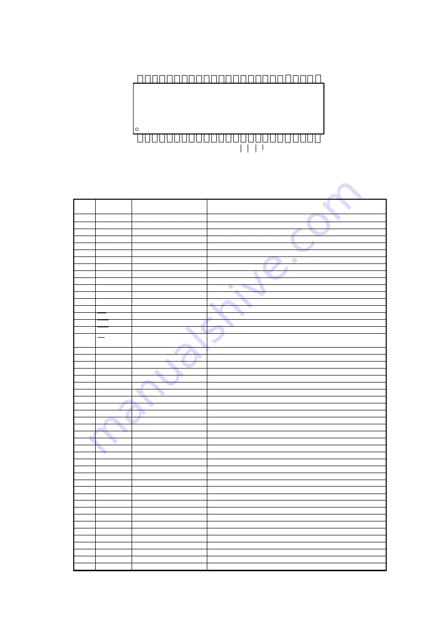
IC402: 16M SDRAM (EM636165TS-7 etc)
1
2
3
4
5
6
7
8
9
10
11
12
13
14
15
16
17
18
19
20
21
42
41
40
39
38
37
36
35
34
33
32
31
30
29
28
27
26
25
24
23
22
43
44
45
46
47
48
49
50
A
9
V
DD
DQ
1
DQ
0
DQ
3
DQ
2
DQ
7
DQ
6
DQ
5
DQ
4
A
0
A
1
A
2
A
3
V
DD
V
SSQ
V
SSQ
LDQM
WE
CAS
RAS
CS
BA
A
10
/AP
V
SS
N.C
CKE
CLK
UDQM
N.C/RFU
V
SSQ
DQ
10
DQ
11
V
DDQ
V
SSQ
DQ
14
DQ
15
V
SS
DQ
13
DQ
12
V
DDQ
DQ
9
DQ
8
A
8
A
7
A
6
A
5
A
4
V
DDQ
V
DDQ
Terminal Function
1
V
DD
Power Supply/Ground
Power and ground for the input buffer and the core logic
2
DQ
0
Data Input/Output
Data input/output are mutiplexed on the same pin
3
DQ
1
Data Input/Output
Data input/output are mutiplexed on the same pin
4
V
SSQ
Data Output Power/Ground
Isolated power supply and ground for the output buffer
5
DQ
2
Data Input/Output
Data input/output are mutiplexed on the same pin
6
DQ
3
Data Input/Output
Data input/output are mutiplexed on the same pin
7
V
DDQ
Data Output Power/Ground
Isolated power supply and ground for the output buffer
8
DQ
4
Data Input/Output
Data input/output are mutiplexed on the same pin
9
DQ
5
Data Input/Output
Data input/output are mutiplexed on the same pin
10
V
SSQ
Data Output Power/Ground
Isolated power supply and ground for the output buffer
11
DQ
6
Data Input/Output
Data input/output are multiplexed on the same pin
12
DQ
7
Data Input/Output
Data input/output are multiplexed on the same pin
13
V
DDQ
Data Output Power/Ground
Isolated power supply and ground for the output buffer
14
L DQM
Data Input/Output Mask
Blocks data input when active
15
WE
Write Enable
Enables write operation and row precharge
16
CAS
Column Address Strobe
Latches column address on the positive going edge of the CLK at low
17
RAS
Row Address Strobe
Latches row address on the positive going edge of the CLK at low
18
CS
Chip Select
Disables or enables device operation by masking or enabling all
inputs except CLK, CKE, and LDQM
19
BA
Bank Select Address
Selects bank to be activated during row address latch time
20
A
10
/AP
Address
Row/column addresses are multiplexed on the same pin
21
A
0
Address
Row/column addresses are multiplexed on the same pin
22
A
1
Address
Row/column addresses are multiplexed on the same pin
23
A
2
Address
Row/column addresses are multiplexed on the same pin
24
A
3
Address
Row/column addresses are multiplexed on the same pin
25
V
DD
Power Supply/Ground
Power and ground for the input buffer and the core logic
26
V
SS
Power Supply/Ground
Power and ground for the input buffer and the core logic
27
A
4
Address
Row/column addresses are multiplexed on the same pin
28
A
5
Address
Row/column addresses are multiplexed on the same pin
29
A
6
Address
Row/column addresses are multiplexed on the same pin
30
A
7
Address
Row/column addresses are multiplexed on the same pin
31
A
8
Address
Row/column addresses are multiplexed on the same pin
32
A
9
Address
Row/column addresses are multiplexed on the same pin
33
N. C
No Connection
No connect pin
34
CKE
Clock Enable
Masks system clock to freeze operation from the next clock cycle
35
CLK
System Clock
Active on the positive going edge to sample all inputs
36
U DQM
Data Input/Output Mask
Blocks data input when active
37
N. C/RFU
NC/Reserved
No connect pin
38
V
DDQ
Data Output Power/Ground
Isolated power supply and ground for the output buffer
39
DQ
8
Data Input/Output
Data input/output are multiplexed on the same pin
40
DQ
9
Data Input/Output
Data input/output are multiplexed on the same pin
41
V
SSQ
Data Output Power/Ground
Isolated power supply and ground for the output buffer
42
DQ
10
Data Input/Output
Data input/output are multiplexed on the same pin
43
DQ
11
Data Input/Output
Data input/output are multiplexed on the same pin
44
V
DDQ
Data Output Power/Ground
Isolated power supply and ground for the output buffer
45
DQ
12
Data Input/Output
Data input/output are multiplexed on the same pin
46
DQ
13
Data Input/Output
Data input/output are multiplexed on the same pin
47
V
SSQ
Data Output Power/Ground
Isolated power supply and ground for the output buffer
48
DQ
14
Data Input/Output
Data input/output are multiplexed on the same pin
49
DQ
15
Data Input/Output
Data input/output are multiplexed on the same pin
50
V
SS
Power Supply/Ground
Power and ground for the input buffer and the core logic
Pin Name
Function
Pin No.
Symbol
3-16
All manuals and user guides at all-guides.com
Содержание SA-11S1
Страница 21: ...1 19 5101 Q102 AT49BV0001AT All manuals and user guides at all guides com a l l g u i d e s c o m...
Страница 24: ...1 22 12 EXPLODED VIEW AND PARTS LIST All manuals and user guides at all guides com...
Страница 38: ...1 36 Personal notes All manuals and user guides at all guides com...
Страница 42: ...Personal notes 2 3 All manuals and user guides at all guides com...
Страница 49: ...IC401 CXD2753R 3 6 All manuals and user guides at all guides com...
Страница 69: ...Super Audio CD MODULE UNIT 4 6 SIGNAL LINE 3 26 All manuals and user guides at all guides com...
Страница 70: ...Super Audio CD MODULE UNIT 5 6 TO 6 6 3 27 All manuals and user guides at all guides com...


