background image

6

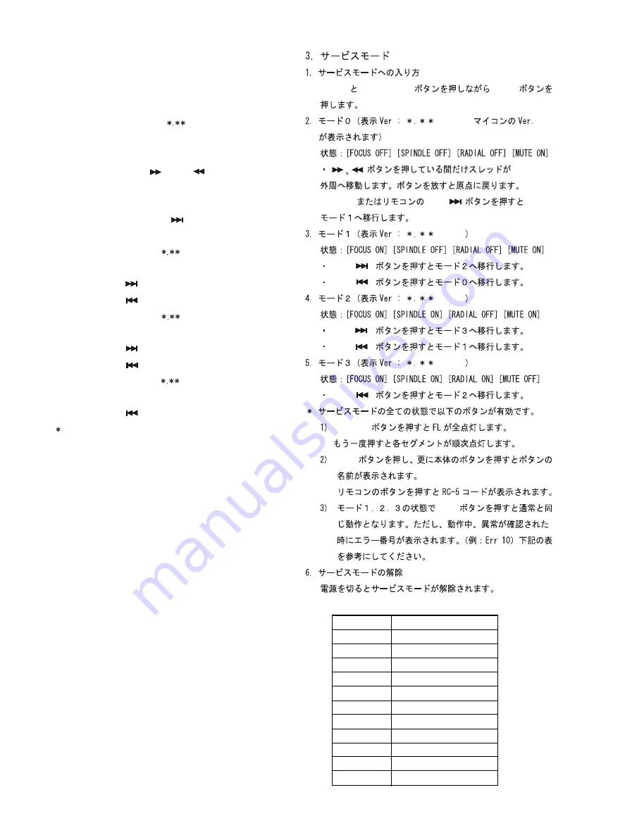
3. SERVICE MODE 

1.  Turning into Service Mode 

While pressing DISPLAY and QUICK  REPLAY buttons, press 

POWER button. 

2. Mode0 

(Display 

:    Ver :         P00  Version number of the 

micro computer is displayed) 

Status: [FOCUS OFF] [SPINDLE OFF] [RADIAL OFF] [MUTE ON] 

• While pressing       and      buttons, the sledge 

moves toward the outer edge. Release the button makes 

the sledge return to the origin. 

Press EASY  JOG or NEXT     button on the remote to go 

to Mode 1. 

3.  Mode 1 (Display : Ver :         P01 

Status: [FOCUS ON] [SPINDLE OFF] [RADIAL OFF] [MUTE ON] 

• Press NEXT     button to go to Mode 2. 

• Press PREV     button to go to Mode 0. 

4.  Mode 2 (Display : Ver :         P02 

Status: [FOCUS ON] [SPINDLE ON] [RADIAL OFF] [MUTE ON] 

• Press NEXT     button to go to Mode 3. 

• Press PREV     button to go to Mode 1. 

5.  Mode 3 (Display : Ver :         P03 

Status: [FOCUS ON] [SPINDLE ON] [RADIAL ON] [MUTE OFF] 

• Press PREV     button to go to Mode 1. 

  In this Service Mode, all of the following button functions 

work in any status. 

1) Press 

DISPLAY

 button to light up all the FL segments. 

Press it again then each FL segment lights up one by 

one. 

2) Press 

STOP

 button. Then press a button on the unit. 

The name of the button is displayed. 

Pressing a button on the remote displays the RC-5 

code of the button. 

3) Press 

PLAY

 button in Mode 1, 2 or 3 then normal 

operation can be performed. If an error occurs the 

error number is displayed. (Ex : Err 10) See the table 

below. 

6.  Terminating Service Mode 

Turn off power to quit Service Mode. 

DISPLAY QUICK  REPLAY

POWER

EASY JOG

NEXT

NEXT

PREV

NEXT

PREV

PREV

DISPLAY

STOP

PLAY

P 0 0

P 0 1

P 0 2

P 0 3

Error Code

Error

Err 02

FOCUS Error

Err 07

SUB CODE Error

Err 08

T. O. C. Error

Err 09

DECODER Error

Err 10

RADIAL Error

Err 11, 12

SLEDGE Error

Err 13

SPINDLE Error

Err 16 ~ 20

SEARCH Error

Err 30

DOOR Error

Err 31

TRAY Error

Err 32 ~ 47

BUTTON INPUT Error

All manuals and user guides at all-guides.com

Содержание CD7300C1G

Страница 1: ...F1N K1G S1G C1G N1G N1B R CD7300 Printed in Japan Please use this service manual with referring to the user guide D F U without fail Service Manual Printed on 100 Recycled Paper DISPLAY OFF PLAY PAUSE...

Страница 2: ...AMAZONIA IND ELET ITDA CENTRO DE INFORMACOES AO CEP 04698 970 SAO PAULO SP BRAZIL PHONE 0800 123123 Discagem Direta Gratuita FAX 55 11 534 8988 JAPAN Technical MARANTZ JAPAN INC 35 1 7 CHOME SAGAMIONO...

Страница 3: ...ital output Coaxial output pin jack 0 5 Vp p 75 ohms Optical output square optical connector 19 dBm Optical readout system Laser AlGaAs semiconductor Wavelength 780 nm Signal system Sampling frequency...

Страница 4: ...the eject pinhole and push the eject lever 2 Use a pin 4mm or less 2 SERVICE PROCEDURE This picture shows the unit upside down The eject lever is pointed by the arrow The lever is thin so aim the narr...

Страница 5: ...with solder Otherwise the laser diode may be damaged by static electricity CD Decorder Board PS01 Repair When Repairing the CD decorder board PS01 you can fix the board on the loader unit as shown in...

Страница 6: ...lose speed Display Default Setting Description Bigger Number Smaller Number T OffTim 003 When open close speed is too fast Note 001 002 003 cannot be set open close speed becomes faster open close spe...

Страница 7: ...e 015 Tray on time 015ms EASYJOG 000 255ms Tray open close Speed open close Speed Tray open close open close speed EASYJOG PUSH ENTER open close speed T OffTim 003 open close speed 000 001 002 open cl...

Страница 8: ...to go to Mode 1 In this Service Mode all of the following button functions work in any status 1 Press DISPLAY button to light up all the FL segments Press it again then each FL segment lights up one b...

Страница 9: ...A7073AT x 3 MOTOR DRIVER SL MOT FO TR POWER SUPPLY CIRCUIT 12V 5VA 8M 5VDAC 3VDAC 3 3V 2 7V 28V AC3 5V 10MHz TZA1024 ADALAS RF AMP LD MON CD TEXT LC89170M SANYO CD ROM MP3 DECODER STA016T 8 43MHz FTD...

Страница 10: ...J801 D813 D814 QN03 QN11 R809 J005 J004 F001 R810 T001 C836 D816 Q808 R811 D815 C835 L829 J010 J009 R883 R882 R881 W803 GND OUT IN GND OUT IN GND OUT IN C B E C B E C B E GND OUT IN C B E C B E GND O...

Страница 11: ...R131 C106 C107 Q106 Q108 R135 Q107 R136 Q112 C132 R150 R149 R148 R142 R146 Q111 R144 R147 C129 R141 C131 R138 R145 Q109 Q110 R139 C133 R137 R140 R143 C130 Q114 R211 Q113 R212 R213 R220 D101 D102 C111...

Страница 12: ...20 19 18 17 50 51 52 53 54 55 56 57 58 59 60 61 62 63 64 2 3 4 5 6 7 8 9 10 11 12 13 14 15 16 47 46 45 44 43 42 41 40 39 38 37 36 35 34 33 TP176 TP178 TP179 TP182 VR 1 2 3 4 5 6 7 14 13 12 11 10 9 8...

Страница 13: ...M2B 100n 100n 100 10 BLM11B252 BLM11B252 BLM11B252 DM DM DM 47P 47P 47P 33P BLM11B601 BLM11B601 100n 47k 47k 10n 10n 4k7 1k 1k 1k 1k DM DM DM DM DM 100P 100P 100P 4n7 4n7 4n7 4n7 10P TC7SHU04 100n DM...

Страница 14: ...3 2 1 TP611 TP616 TP918 5 3 6 7 1 2 4 3 1 2 3 1 2 3 1 2 3 1 2 1 3 2 1 3 2 1 3 2 1 3 2 1 3 2 1 3 2 1 3 2 1 3 2 3 5 2 1 7 6 4 1 2 3 1 3 2 1 3 2 1 2 3 1 2 3 1 3 2 1 2 3 1 3 2 1 2 3 1 2 3 1 2 3 1 2 3 1 2...

Страница 15: ...2 1 1 2 3 4 5 6 7 8 TPY06 TPY05 TPY10 TPY09 TPY07 TPY08 TPY16 TPY18 TPY13 TPY15 TPY11 TPY12 TPY17 TPY19 TPY20 TPY01 TPY02 20 19 18 17 16 15 14 13 12 11 10 9 8 7 6 5 4 3 2 1 1 2 3 TPY24 TPY23 TPY21 TP...

Страница 16: ...TPF18 AC1 AC2 28V 5VD 1 2 1 2 1 2 1 2 1 2 1 2 1 2 4 2 1 5 3 1 2 1 2 1 2 1 2 1 2 1 2 1 2 1 2 1 2 1 3 2 TPF20 TPF21 TPF22 TPF24 TPF23 TPF26 TPF27 TPF25 TPF28 TPF30 TPF36 TPF31 TPF34 TPF33 TPF35 TPF29 TP...

Страница 17: ...Even D402 D406 Even Q401 Q409 Odd D401 D405 Odd QD01 QD02 QD03 QN04 QN05 Q808 D815 QN06 QN07 Q805 Q801 Q807 D810 D813 Q802 Q803 D814 Q411 Q427 Q414 Q412 Q604 Q603 Q602 Q613 D801 D804 D805 D806 DN01 D...

Страница 18: ...05 Q112 Q114 Q113 Q101 Q106 108 Q102 Q103 Q111 Q109 D102 Q110 D101 Q150 Q152 Q154 Q153 QY02 QY01 Q201 QY03 QM01 QM02 DR02 QR21 Q104 PS01 QR01 DR01 QR02 DF02 PF01 All manuals and user guides at all gui...

Страница 19: ...mon ModeS Voltage See Description M0 SDA CDOUT AOUTL Differential Output Digital Ground DGND AOUTL Differential Output Digital Power VD VA Analog Power Digital Power VD AGND Analog Ground Digital Grou...

Страница 20: ...nterface left right Clock To DAC 22 SDO O DAC serial data To DAC 21 BCKO O DAC bit clock To DAC 19 OSCK O DAC oversampling clock To DAC ADC GPSO interface 55 GPSO_CK I GPSO bit clock From MCU 54 GPSO_...

Страница 21: ...LINK 63 SCL I I2C clock signal From MCU 64 SDA I O I2C data signal To MCU MISCELLANEOUS 17 XTI I Oscillator input 18 XTO O Oscillator output 25 CLKOUT O Buffered output clock 15 RESET I Reset 16 TESTE...

Страница 22: ...output programmable open drain VSSD1 33 1 digital ground 2 V2 V3 34 versatile I O input versatile pin 2 or output versatile pin 3 open drain WCLI 35 word clock input for data loopback to DAC SDI 36 se...

Страница 23: ...0 A0 O n c L n c 49 P81 A1 O n c L n c 50 P82 A2 O n c L n c 51 P83 A3 O n c L n c 52 P84 A4 O n c L n c 53 P85 A5 O n c L n c Pin No Port Name I O Signal Name Pull up Initial Remarks 54 P86 A6 O n c...

Страница 24: ...9 0 7 0 G 5 1 2 8 3 x 8 M x 2 PP 0 1 5 1 2 9 3 x 8 M x 1 5 1 2 7 3 x 8 M x 3 5 1 2 9 3 x 8 M x 1 5 1 2 8 2 x 6 M x 1 5 1 2 9 3 x 8 M x 2 5 1 2 8 3 x 8 M x 1 0 3 1 B 0 3 0 B 5 1 2 8 3 x 8 M x 1 0 4 0 G...

Страница 25: ...T154250 KNOB HEADPHONE VOLUME GOLD 284T154250 050B BLACK 05AK270010 BUTTON POWER BLACK 05AK270010 050B GOLD 05AK270110 BUTTON POWER GOLD 05AK270110 009G 183J057010 LEG GOLD HOT STAMP FRONT 183J057010...

Страница 26: ...36 POS NO VERS COLOR PART NO FOR EUR DESCRIPTION PART NO MJI 1 QP40410986 SUSPENSION 4822 404 10986 QP40410986 2 QP40111709 CLAMPER 4822 401 11709 QP40111709 3 QP35810266 BELT 4822 358 10266 QP358102...

Страница 27: ...71 2200 pF 222 C 5 ELECTROLY CAP 6 FILM CAP 5 EA 10 Electrolytic capacitor One way lead type Tolerance 20 Examples Capacity value 0 1 F 104 4 7 F 475 100 F 107 0 33 F 334 10 F 106 330 F 337 1 F 105 22...

Страница 28: ...00 C902 nsp CER CHIP 220pF DK96221300 C903 nsp ELECT 100 F M 16V RA 2 OA10701620 C904 nsp ELECT 100 F M 16V RA 2 OA10701620 PH01 RESISTORS R901 RM01031170 VARIABLE RK09L12B0 10K B D CUT REVERSE RM0103...

Страница 29: ...R327 nsp CHIP 1k 5 1 16W NN05102610 R328 nsp CHIP 1k 5 1 16W NN05102610 R333 nsp CHIP 10k 5 1 16W NN05103610 R334 nsp CHIP 10k 5 1 16W NN05103610 R401 nsp CHIP 1k 5 1 16W NN05102610 R406 R407 nsp CHI...

Страница 30: ...2 HC3890909F IC REG NJM7809FA 9V 1A HC3890909F Q803 HC3990909F IC REG NJM7909FA HC3990909F Q805 HT417622B0 TRS 2SD1762 E F HT417622B0 Q806 HC39124090 IC REG NJM79L24A 0 1A 24V HC39124090 Q807 HC381050...

Страница 31: ...00 CM11 nsp CER CHIP 1 F 10V F DK98105200 CM13 nsp CER CHIP 4700pF 10 B 50V DK96472300 CM14 nsp CER CHIP 470pF DK96471300 CM15 nsp CER CHIP 1 F 10V F DK98105200 CM16 nsp CER CHIP 0 1 F GRM39F104Z16 DK...

Страница 32: ...CHIP 10k 5 1 16W NN05103610 RR22 nsp CHIP 2 2k 5 1 16W NN05222610 RR23 nsp CHIP 10k 5 1 16W NN05103610 RY01 nsp CHIP 47k 5 1 16W NN05473610 RY02 nsp CHIP 10 5 1 16W NN05100610 RY03 nsp CHIP 47k 5 1 1...

Страница 33: ...1 TRANS CIRCUIT BOARD J007 K nsp PLUG B3P5 VH YP04000920 J007 C F N S YP04000760 PLUG CONNECTOR 2P B3P VH YP04000760 T001 F nsp MAINS TRANSF EI57 25 100V 50 60HZ TS15725190 T001 K nsp MAINS TRANSF EI5...

Отзывы: