


Information Manual
DSP1611/17/18/27/28/29 DIGITAL SIGNAL PROCESSOR
April 1998
Serial I/O
Lucent Technologies Inc.
DRAFT COPY
7-19
7.6 Multiprocessor Mode Description
(continued)
7.6.2 Detailed Multiprocessor Mode Description (continued)
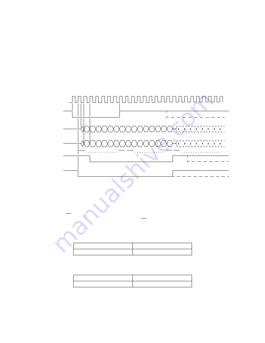
shows the timing when a DSP drives the multiprocessor bus for any particular time slot. The timing is
similar to active mode 16-bit output. The difference is ADD and DO are driven for only one-half cycle during the
transmission of the first bit to prevent bus conflicts if the bus drive is switched from one DSP to another on time slot
boundaries. The DOEN pin is bidirectional in multiprocessor mode and is driven low during each time slot in which
the particular DSP is an output. This signal is not required externally for multiprocessor mode but is used internally
by the DSP and can also be useful to the hardware designer in some applications.
5-4127
Figure 7-16. Multiprocessor Mode Output Timing
Whenever a DSP drives the bus in some time slot, the address of the destination DSP(s) is sent out on the ADD
line concurrent with the transmission of the first 8 bits of the data. The bits of the address are inverted. This desti-
nation address (
[7:0]) consists of the transmit address field of the srta register (bits 7—0) in the transmitting
device. Following this transmission, protocol information (
[7:0]) from the transmitting DSP is sent out on the
ADD line concurrent with the transmission of the last 8 bits of the data. This protocol information is obtained from
the low byte of the saddx register (bits 7—0) and can be written with any arbitrary value. The high byte of saddx is
ignored on a write:
This 8-bit protocol information will be latched into the high byte of saddx by all receiving DSPs with matching
address, and this information is made available to the software by reading the saddx register:
Bit
15—8
7—0
Write to saddx
X
AS[7—0]
(Transmitted AS)
Bit
15—8
7—0
Read from saddx
AS[7—0]
0
(Received AS)
OLD
DO
SADD
OSE
DOEN
AD0
AD7 AS0
AS7
OCK
D0 D1
D15
AD0
D0 D1
AD
AS
Содержание DSP1611
Страница 18: ...Chapter 1 Introduction...
Страница 27: ...Chapter 2 Hardware Architecture...
Страница 52: ...Chapter 3 Software Architecture...
Страница 116: ...Chapter 4 Instruction Set...
Страница 154: ...Chapter 5 Core Architecture...
Страница 176: ...Chapter 6 External Memory Interface...
Страница 208: ...Chapter 7 Serial I O...
Страница 237: ...Chapter 8 Parallel I O DSP1617 Only...
Страница 261: ...Chapter 9 Parallel Host Interface PHIF DSP1611 18 27 28 29 Only...
Страница 275: ...Chapter 10 Bit I O Unit...
Страница 284: ...Chapter 11 JTAG Test Access Port...
Страница 306: ...Chapter 12 Timer...
Страница 313: ...Chapter 13 Bit Manipulation Unit...
Страница 325: ...Chapter 14 Error Correction Coprocessor DSP1618 28 Only...
Страница 350: ...Chapter 15 Interface Guide...
Страница 367: ...Appendix A Instruction Encoding...
Страница 379: ...Appendix B Instruction Set Summary...
Страница 381: ...aD extractz aS IM16 B 52 aD insert aS arM B 53 aD insert aS IM16 B 54 aD aS aaT B 55...
Страница 437: ...Index...