


363-206-295
Circuit Pack Descriptions
7-20
Issue 1
December 1997
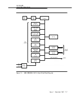
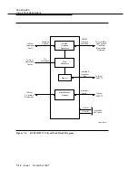
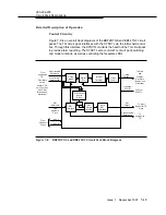
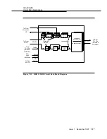
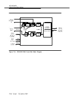
Timing Circuitry
7
DS1 External Timing.
7
Each TG circuit pack receives one DS1 reference signal
which it monitors and from which it recovers a clock signal. The recovered clock is
cross-fed to its companion TG circuit pack in the same shelf. If the microprocessor
on one TG circuit pack detects an incoming DS1 reference failure, it will signal the
microprocessor on the companion TG circuit pack. Thus, each TG circuit pack has
two DS1 references to choose from, one which is input directly and the other
cross-fed. Both TG circuit packs will normally select the same DS1 input. A loss of
both DS1 references will result in the TG circuit pack entering holdover mode.
Line Timing.
7
The reference signal feeding the phase-locked loop is selected
from the internal oscillator or a loop-timing clock derived from the incoming optical
line. In line (formerly loop)-timing mode, the OC-N line being selected for
transmission is also selected as the timing reference. Loss of both line timing
references will cause the TG circuit pack to go into holdover mode to maintain
system timing.
Free-Running.
7
For free-running operation, the TG derives timing from a
temperature-compensated, voltage-controlled crystal oscillator (TCVCXO) and a
digital phase-locked loop (DPLL) with a full temperature range end-of-life
accuracy of
±
15 parts-per-million (ppm) for the BBF2B TGS, and
±
4.6 ppm for the
BBF4 TG3.
DS1 Output.
7
The DS1 output port of the TG circuit pack can be provisioned for
either MULT or SYNC OUT mode via a hardware switch. In the SYNC OUT mode,
the derived DS1 output signal is generated from the incoming OC-N lines through
timing synchronization signals from the DDM-2000 OC-12 main OLIUs (main-b-1
or main-b-2), which is the default. In the MULT mode, the DS1 output signal is
buffered from an external DS1 input reference. This external reference is typically
a DS1 from a building integrated timing supply (BITS).
Selection of these timing synchronization signals for the DS1 output in SYNC
mode is controlled by the SYSCTL circuit pack. This selection can be provisioned
via software command to "track" the active received side of the OC-N line used for
transmission, to always select its timing from the specified OC-12 line (main-b-1
or main-b-2) regardless of its maintenance condition. Loss of timing reference for
the DS1 output will result in the insertion of DS1 AIS on this output port.
Holdover.
7
The TG circuit pack has an internal TCVCXO that will maintain shelf
timing in the event of an unprotected timing DS1 reference failure (that is, holdover
mode). The TGS (BBF2B) will maintain frequency stability to better than a SONET
minimum clock (SMC) accuracy. The TG3 (BBF4) will maintain frequency stability
to better than a stratum 3 accuracy. Beyond this 24 hour period holdover will
gradually return to a free-run accuracy.
Содержание DDM-2000 OC-12
Страница 1: ...363 206 295 Issue 1 December 1997 DDM 2000 OC 12 Multiplexer Release 7 0 User Service Manual Volume I ...
Страница 37: ...Tables xxxviii Issue 1 December 1997 A A SONET Overview A 1 SONET Payloads A 18 A 2 SONET Transport Rates A 19 ...
Страница 506: ...INS PROG 8 of 8 Page INS PROG COMMANDS RELATED rtrv eqpt rtrv ne OC 12 DDM 2000 1997 December 1 Issue 11 89 ...
Страница 528: ...RTRV ATTR ALM 2 of 2 Page RTRV ATTR ALM COMMANDS RELATED set attr alm OC 12 DDM 2000 1997 December 1 Issue 11 111 ...
Страница 565: ...RTRV OC3 3 of 3 Page RTRV OC3 COMMANDS RELATED rtrv sync 11 148 1997 December 1 Issue OC 12 DDM 2000 ...
Страница 664: ...SET FEAT 3 of 3 Page SET FEAT COMMANDS RELATED rtrv feat OC 12 DDM 2000 1997 December 1 Issue 11 247 ...
Страница 766: ... Ctl T TOGGLE 2 of 2 Page Ctl T TOGGLE COMMANDS RELATED logout rlgn OC 12 DDM 2000 1997 December 1 Issue 11 349 ...
Страница 847: ...Multiplexer OC 12 DDM 2000 7 Release TARP TOP Manual User Service II Volume 363 206 295 1 Issue 1997 December ...
Страница 867: ...363 206 295 TOP Maintenance and Operation BLANK LEFT INTENTIONALLY PAGE THIS 12 1997 December 1 Issue ...
Страница 1145: ...Order Circuit 363 206 295 NTP 029 1 of 1 Page 1997 December 1 Issue Unused LISTED ORDER IN BELOW ITEMS DO TO GO DETAILS FOR ...
Страница 1146: ...Order Circuit 363 206 295 NTP 030 1 of 1 Page 1997 December 1 Issue Unused LISTED ORDER IN BELOW ITEMS DO TO GO DETAILS FOR ...
Страница 1182: ...Turnup System 363 206 295 NTP 033 1 of 1 Page 1997 December 1 Issue Unused LISTED ORDER IN BELOW ITEMS DO TO GO DETAILS FOR ...
Страница 1243: ...Clearing Trouble 363 206 295 TAP 107 1 of 1 Page 1997 December 1 Issue Unused ...
Страница 1393: ...363 206 295 DLP 513 1 of 1 Page 1997 December 1 Issue Unused ...
Страница 1394: ...363 206 295 DLP 514 1 of 1 Page 1997 December 1 Issue Unused ...
Страница 1456: ...363 206 295 DLP 523 7 of 7 Page 1997 December 1 Issue OC 12 via Access Broadcast Video for Cross connections of Example 4 Figure ...
Страница 1465: ...DLP 525 363 206 295 1997 December 1 Issue 6 of 2 Page Schematic Ring Virtual ATM Sample 1 Figure ...
Страница 1469: ...DLP 525 363 206 295 1997 December 1 Issue 6 of 6 Page Ring Virtual ATM OC 12 DDM 2000 for Cross connections of Example 4 Figure ...
Страница 1565: ...363 206 295 DLP 543 6 of 5 Page 1997 December 1 Issue Network Broadcast Video of Test Transmission 2 Figure ...
Страница 1566: ...DLP 543 363 206 295 1997 December 1 Issue 6 of 6 Page Network Ring Virtual ATM of Test Transmission 3 Figure ...