L
X
Y
2
8
1
6
U
S
E
R
’
M
A
N
SHENZHEN LINGXINYU SCIENCE AND TECHNOLOGY CO., LTD
16
Страница 1: ...NU UA AL L S SH HE EN NZ ZH HE EN N L LI IN NG GX XI IN NY YU U S SC CI IE EN NC CE E A AN ND D T TE EC CH HN NO OL LO OG GY Y C CO O L LT TD D 1 L LX XY Y2 28 81 16 61 1 U US SE ER R S S M MA AN NU UA AL L JULY 2008 V1 0 Pay attention to the last page ...
Страница 2: ...s 8 2 6 Timing Waveform 9 2 6 1 Serial Port Timing Waveform 9 2 6 2 Output Current Channel Timing Waveform 9 2 7 Constant Current 10 2 8 Setting Output Current 10 2 9 Delay Time of Staggered Output 10 2 10 Package Power Dissipation 10 2 11 Usage of Thermal Pad 10 2 12 Thermal Protection Function 11 2 13 LED Supply Voltage 11 2 14 Switching Noise Reduction 11 2 15 Equivalent Circuits of Inputs and ...
Страница 3: ...atures z Backward compatible with main trend 16 channel constant current IC in package z 16 constant current output channels z 16 bit color depth W PWM control z Refresh rate up to 4800Hz z Schmitt trigger input z Staggered output delay reduce EMI z Over temperature protection z Constant output current range 5V 5 60mA z Output current accuracy between channels 3 between ICs 6 z Maximum data clock ...
Страница 4: ... 81 16 61 1 U US SE ER R S S M MA AN NU UA AL L S SH HE EN NZ ZH HE EN N L LI IN NG GX XI IN NY YU U S SC CI IE EN NC CE E A AN ND D T TE EC CH HN NO OL LO OG GY Y C CO O L LT TD D 4 Block Diagram Pin Configuration ...
Страница 5: ...t driver IC R EXT 23 Controlling Input terminal used to connect an external resistor for setting up output current for all output channels VDD 24 Power 5V supply voltage terminal 2 2 Maximum Rating Characteristic Symbol Rating Unit Supply Voltage VDD 7 V Input Pin Voltage SDI VIN 0 4 VDD 0 4 V Output Current IOUT 60 mA Sustaining Voltage at OUT Port VDS 7 V Data Clock Frequency DCLK 25 MHz GND Ter...
Страница 6: ...DD V Output Leakage Current IOH VDS 7 0V 0 5 μA VOL IOL 6 0mA 0 4 V Output Voltage SDO VOH IOH 6 0mA 4 6 V Current Skew Channel ΔIOUT 1 IOUT 10 8mA VDS 1 0V Rext 1800Ω 1 5 3 0 Current Skew IC ΔIOUT 2 IOUT 10 8mA VDS 1 0V Rext 1800Ω 3 0 6 0 Output Current vs Output Voltage Regulation ΔV DS VDS 1 0V and 3 0V Rext 910Ω 21mA 0 1 0 5 V Output Current vs Output Voltage Regulation dV DD VDD 4 5V and 5 5V...
Страница 7: ...VDD VIL GND DCLK output to the receiver end SDI of next driver IC Propagation Delay Time GCLK OUT4n tPD1 75 ns OUT4n 1 tDL1 25 ns OUT4n 2 tDL2 50 ns Stagger Delay Time OUT4n 3 tDL3 75 ns LE tw L 5 ns Pulse Width DCLK tw DCLK 20 ns Output Rise Time of Output Ports tOR 10 20 ns Output Fall Time of Output Ports tOF RL 152Ω CL 10pF C1 100nF C2 10μF 10 20 ns Refer to the Timing Waveform when n 0 1 2 3 ...
Страница 8: ...61 1 U US SE ER R S S M MA AN NU UA AL L 2 5 Test Circuit for Switching Characteristics S SH HE EN NZ ZH HE EN N L LI IN NG GX XI IN NY YU U S SC CI IE EN NC CE E A AN ND D T TE EC CH HN NO OL LO OG GY Y C CO O L LT TD D 8 ...
Страница 9: ... AN NU UA AL L 2 6 Timing Waveform 2 6 1 Serial Port Timing Waveform 2 6 2 Output Current Channel Timing Waveform S SH HE EN NZ ZH HE EN N L LI IN NG GX XI IN NY YU U S SC CI IE EN NC CE E A AN ND D T TE EC CH HN NO OL LO OG GY Y C CO O L LT TD D 9 ...
Страница 10: ...8mA when Rext 1800Ω 2 9 Delay Time of Staggered Output LXY28161 has a built in staggered circuit to perform delay mechanism 16 channels are divided to four groups Each output port has 25nS delay time so that the instant current from the power line will be lowered 2 10 Package Power Dissipation The maximum allowable package power dissipation is determined as PD max Tj Ta Rth j a When 16 output chan...
Страница 11: ...PD act PD max when VLED 5V and VDS VLED VF in which VLED is the load supply voltage In this case it is recommended to use the lowest possible supply voltage or to set an external voltage reducer VDROP A voltage reducer lets VDS VLED VF VDROP Resistors or Zener diode can be used in the applications as shown in the following figures S SH HE EN NZ ZH HE EN N L LI IN NG GX XI IN NY YU U S SC CI IE EN ...
Страница 12: ... Inputs and Outputs Equivalent circuits of Inputs and Outputs 3 Package Outline LXY2816 applies SOP 24 and TSSOP 24 package outline S SH HE EN NZ ZH HE EN N L LI IN NG GX XI IN NY YU U S SC CI IE EN NC CE E A AN ND D T TE EC CH HN NO OL LO OG GY Y C CO O L LT TD D 12 SOP 24 Outline Drawing ...
Страница 13: ...2 28 81 16 61 1 U US SE ER R S S M MA AN NU UA AL L S SH HE EN NZ ZH HE EN N L LI IN NG GX XI IN NY YU U S SC CI IE EN NC CE E A AN ND D T TE EC CH HN NO OL LO OG GY Y C CO O L LT TD D 13 SSOP 24 Outline Drawing ...
Страница 14: ...uld satisfy Rt Rf N 9 besides set the value as small as possible Otherwise there will be current difference between ICs which will effect the color uniformity S SH HE EN NZ ZH HE EN N L LI IN NG GX XI IN NY YU U S SC CI IE EN NC CE E A AN ND D T TE EC CH HN NO OL LO OG GY Y C CO O L LT TD D 14 ...
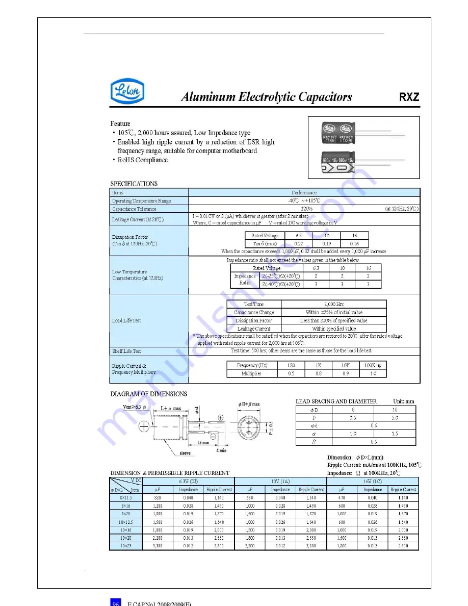
Страница 15: ... that suit most In out test 3 3V is good 4 3 For Electronic capacitors please use Taiwan Lelon s RXZ series high frequency capacitors or some other brand which is similar in functions with the follow specifications S SH HE EN NZ ZH HE EN N L LI IN NG GX XI IN NY YU U S SC CI IE EN NC CE E A AN ND D T TE EC CH HN NO OL LO OG GY Y C CO O L LT TD D 15 http www lelon com tw index php fn search2 keywor...
Страница 16: ...L LX XY Y2 28 81 16 61 1 U US SE ER R S S M MA AN NU UA AL L SHENZHEN LINGXINYU SCIENCE AND TECHNOLOGY CO LTD SHENZHEN LINGXINYU SCIENCE AND TECHNOLOGY CO LTD 16 ...