Linear Technology LTC1624 Скачать руководство пользователя страница 19

19

LTC1624

where

I

V

V

V

V

OUT MAX

IN

OUT

D

IN

:

 I

SW MAX

( )

( )

=

+

+

δ

 is the temperature dependency of R

DS(ON)

 and k is a

constant inversely related to the gate drive current. The
maximum switch current occurs at V

IN(MIN)

 and the peak

switch current is I

SW(MAX) 

+

 ∆

I

L

/2. The maximum voltage

across the switch is V

IN(MAX) 

V

OUT

.

MOSFETs have I

2

R losses plus the P

MAIN

 equation

includes an additional term for transition losses that are
highest at high total input plus output voltages. For
(

V

OUT

+ V

IN

) < 20V the high current efficiency generally

improves with larger MOSFETs, while for (

V

OUT

+ V

IN

)

> 20V the transition losses rapidly increase to the point
that the use of a higher R

DS(ON) 

device with lower C

RSS

actual provides higher efficiency. For additional informa-
tion refer to the Step-Down Converter: Power MOSFET
Selection in the Applications Information section.

Positive-to-Negative Converter: Inductor Selection

For most applications the inductor will fall in the range of
10

µ

H to 100

µ

H. Higher values reduce the input and output

ripple voltage (although not as much as step-down con-
verters) and also reduce core loss. Lower inductor values
are chosen to reduce physical size and improve transient
response but do increase output ripple.

Like the boost converter, the input current of the positive-
to-negative converter is calculated at full load current.
Peak inductor current can be significantly higher than
output current, especially with smaller inductors (with
high 

I

L

 values). The following formula assumes continu-

ous mode operation and calculates maximum peak induc-
tor current at minimum V

IN

:

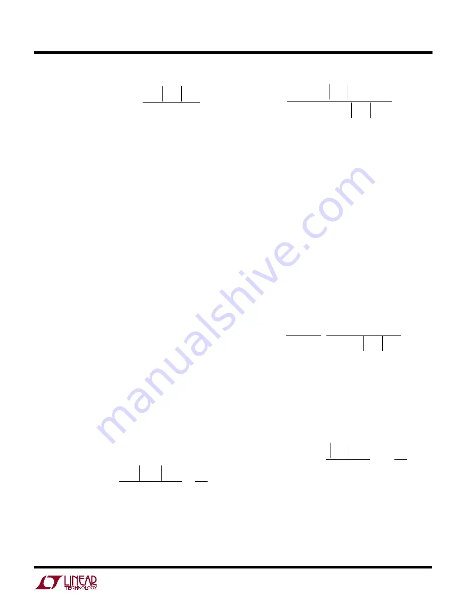
I

I

V

V

V

V

I

L PEAK

OUT MAX

IN

OUT

D

IN

L

( )

( )

=

+

+

+

2

The ripple current in the inductor (

I

L

) is typically 20% to

50% of the peak inductor current occuring at V

IN(MIN)

 and

I

OUT(MAX)

 to minimize output ripple. Maximum 

I

L

 occurs

at minimum V

IN

.

APPLICATIO

N

S I

N

FOR

M

ATIO

N

W

U

U

U

I

V

V

V

kHz L V

V

V

L

IN

OUT

D

IN

OUT

D

P-P

( )

=

( )

+

(

)

(

)( )

+

+

(

)

200

Specify the maximum inductor current to safely handle
I

L(PEAK)

. Make sure the inductor’s saturation current rat-

ing (current when inductance begins to fall) exceeds the
maximum current rating set by R

SENSE

.

Positive-to-Negative Converter: R

SENSE 

Selection for

Maximum Output Current

R

SENSE

 is chosen based on the required output current.

Remember the LTC1624 current comparator has a maxi-
mum threshold of 160mV/R

SENSE

. The current compara-

tor threshold sets the peak of the inductor current, yielding
a maximum average output current I

OUT(MAX)

 equal to

I

L(PEAK)

 less half the peak-to-peak ripple current with the

remainder divided by the duty cycle.

Allowing a margin for variations in the LTC1624 (without
considering variation in R

SENSE

) and assuming 30% ripple

current in the inductor, yields:

R

mV

I

V

V

V

V

SENSE

OUT MAX

IN MIN

IN MIN

OUT

D

=

+

+

( )

( )

( )

100

Positive-to-Negative Converter: Output Diode

The output diode conducts current only during the switch
off-time. Peak reverse voltage for positive-to-negative
converters is equal to 

V

OUT

+ V

IN

. Average forward

current in normal operation is equal to I

D(PEAK) 

 ∆

I

L

/2.

Peak diode current (occurring at V

IN(MIN)

) is:

I

I

V

V

V

I

D PEAK

OUT MAX

OUT

D

IN

L

( )

( )

=

+

(

)

+

+

1

2

Positive-to-Negative Converter: Input and
Output Capacitors

The output capacitor is normally chosen by its effective
series resistance (ESR), because this is what determines
output ripple voltage. Both input and output capacitors
need to be sized to handle the ripple current safely.

Содержание LTC1624

Страница 1: ...oost step down inverting and SEPIC Burst ModeTM operation provides high efficiency at low load currents A maximum highdutycyclelimitof95 provideslowdropoutoperation whichextendsoperatingtimeinbattery...

Страница 2: ...Regulation VIN 3 6V to 20V Note 2 0 002 0 01 V VLOAD REG Output Voltage Load Regulation Note 2 ITH Sinking 5 A 0 5 0 8 ITH Sourcing 5 A 0 5 0 8 VOVL Output Overvoltage Lockout 1 24 1 28 1 32 V IQ Inpu...

Страница 3: ...ge Boost Line Regulation INPUT VOLTAGE V 0 BOOST VOLTAGE V 6 5 4 3 2 1 0 15 25 1624 G04 5 10 20 30 35 IBOOST 1mA VSW 0V BOOST LOAD CURRENT mA 0 BOOST VOLTAGE V 6 5 4 3 2 1 0 15 25 1624 G06 5 10 20 30...

Страница 4: ...0 10 60 85 1448 G12 15 35 110 135 VOUT IN REGULATION VFB 0V PIN FUNCTIONS U U U SENSE Pin 1 Connects to the input for the current comparator Built in offsets between the SENSE and VIN pinsinconjunctio...

Страница 5: ...charged during each off cycle The dropout detector counts the number of oscillator cycles that the top MOSFET remains on and periodically forces a brief off period to allow CB to recharge Themaincontr...

Страница 6: ...RIVER TG SW D1 L1 N CHANNEL MOSFET N CHANNEL MOSFET INTV CC R SENSE SENSE D B 5 6V INTV CC REG V IN 0 8V 1 19V 200kHz 200kHz 1 19V I TH RUN 1 28V 1 19V 180k 1 5V 3 A 30k 8k 2 3 4 5 6 7 GND 1624 FD 2 5...

Страница 7: ...esults in higher output voltage ripple and greater core losses A reasonable starting point for setting ripple current is IL 0 4 IMAX Remember the maximum IL occurs at the maximum input voltage The ind...

Страница 8: ...eterm 1 isgenerallygivenforaMOSFETintheform of a normalized RDS ON vs Temperature curve but 0 005 C can be used as an approximation for low voltageMOSFETs CRSSisusuallyspecifiedintheMOSFET APPLICATION...

Страница 9: ...will be scaled by a factor of Duty Cycle Efficiency For 5V regulators this simply means connecting the BOOST monlyusedfordesignbecauseevensignificantdeviations donotoffermuchrelief Notethatcapacitorma...

Страница 10: ...at approximately 10mV RSENSE at VITH RUN 1 4V and ends at 160mV RSENSE VITH RUN 2 4V The output current thus ramps up slowly charging the outputcapacitor Thepeakinductorcurrentandmaximum output curren...

Страница 11: ...ed in the sense resistor only when the topside MOSFET is on The I2R loss is thus reduced by the duty cycle For example at 50 DC if RDS ON 0 05 RL 0 15 and RSENSE 0 05 then the effective total resistan...

Страница 12: ...Note that the transient suppressor should not conduct during double battery operation but must still clamptheinputvoltagebelowbreakdownoftheconverter Although the LTC1624 has a maximum input voltage o...

Страница 13: ...VIN In this case the worst case dissipation rises to P I V V V V D SC AVG D IN IN D APPLICATIONS INFORMATION W U U U With the 0 05 sense resistor ISC AVG 2A will result increasing the 0 5V Schottky di...

Страница 14: ...the peak inductor current occuring at VIN MIN and IOUT MAX I V V V V kHz L V V L IN OUT D IN OUT D P P 200 with IL MAX IL P P at VIN VIN MIN Remember boost converters are not short circuit pro tected...

Страница 15: ...The input voltage source imped ance determines the size of the capacitor that is typically 10 F to 100 F A low ESR is recommended although not as critical as the output capacitor and can be on the or...

Страница 16: ...tional term for transition losses that are highest at high total input plus output voltages For VIN VOUT 20V the high current efficiency generally improves with larger MOSFETs while for VIN VOUT 20V t...

Страница 17: ...UT D IN MIN L 1 1 Schottky diodes such as MBR130LT3 are recommended SEPIC Converter Input and Output Capacitors The output capacitor is normally chosen by its effective series resistance ESR because t...

Страница 18: ...h Duty Cycle V V OUT IN with VOUT being the absolute value of VOUT The MOSFET power dissipation and maximum switch current are given by that the voltage across C1 is constant such that VC1 VIN at full...

Страница 19: ...N I I V V V V I L PEAK OUT MAX IN OUT D IN L 2 The ripple current in the inductor IL is typically 20 to 50 of the peak inductor current occuring at VIN MIN and IOUT MAX to minimize output ripple Maxim...

Страница 20: ...624 ground pin referenced to VOUT the nonimal range on the ITH RUN pin is VOUT in shutdown to VOUT 2 4V at Max IOUT Referring to Figure15 M2 M3andR3providealevelshiftfromtypical TTL levels to the LTC1...

Страница 21: ...8 7 6 5 1 2 3 4 R2 35 7k 1 R1 11k 1 COUT 100 F 10V 2 M1 Si4412DY L1 10 H RSENSE 0 033 CIN 22 F 35V 2 VOUT 5V 3A VIN 5 3V TO 28V 1624 F10 COILTRONICS CTX10 4 0 1 F Figure 10 5V 3A Converter with Outpu...

Страница 22: ...ST TG SW LTC1624 1000pF 100pF CC 470pF RC 6 8k D1 MBRS140T3 CB 0 1 F 8 7 6 5 1 2 3 4 R2 35 7k 1 R1 3 92k 1 COUT 100 F 16V 2 M1 Si4412DY L1 47 H RSENSE 0 068 CIN 22 F 35V 2 VOUT 12V 1A VIN 12 3V TO 28V...

Страница 23: ...F 8 7 6 5 1 2 3 4 R2 35 7k 1 R1 20k 1 COUT 100 F 10V 2 M1 Si6426DQ L1 20 H RSENSE 0 068 CIN 22 F 35V 2 VOUT 3 3V 1 5A VIN 3 5V TO 18V 1624 F16 COILTRONICS CTX20 4 0 1 F Figure 16 Low Dropout 3 3V 1 5A...

Страница 24: ...12V 10A Buck Converter with Output Derived Boost Voltage SENSE ITH RUN VFB GND VIN BOOST TG SW LTC1624 CIN1 CIN2 1000 F 35V 2 VIN 13V TO 28V D1 CB 0 1 F C5 3 3 F 50V C4 0 1 F 8 7 6 5 1 2 3 4 RSENSE2...

Страница 25: ...MOTOROLA MBR2535CT L1 MAGNETICS CORE 55930AZ WINDING 8T 14BIF M1 INTERNATIONAL RECTIFIER IRL 3803 RSENSE IRC OAR 3 0 005 5 BOTH D1 AND Q1 MOUNTED ON THERMALLOY MODEL 6399 HEAT SINK SENSE ITH RUN VFB...

Страница 26: ...RRENT ADJ R2 35 7k RC 10k CC 330pF M1 COUT 100 F 16V 2 L1 27 H R4 0 025 VOUT 12V 3A 1624 F21 CIN1 CIN2 KEMET T495X226M035AS L1 SUMIDA CDRH127 270 RSENSE IRC LR2010 01 R033 F R4 IRC LR2010 01 R025 F M1...

Страница 27: ...2 0 014 0 019 0 355 0 483 0 004 0 010 0 101 0 254 0 050 1 270 TYP DIMENSION DOES NOT INCLUDE MOLD FLASH MOLD FLASH SHALL NOT EXCEED 0 006 0 152mm PER SIDE DIMENSION DOES NOT INCLUDE INTERLEAD FLASH IN...

Страница 28: ...LT 1375 LT1376 1 5A 500kHz Step Down Switching Regulators High Frequency LTC1433 LTC1434 Monolithic 0 45A Low Noise Current Mode Step Down Switching Regulators 16 and 20 Pin Narrow SSOP LTC1435 High...

Отзывы: