


7
DEMO MANUAL DC257
NO-DESIGN SWITCHER
OPERATIO
U
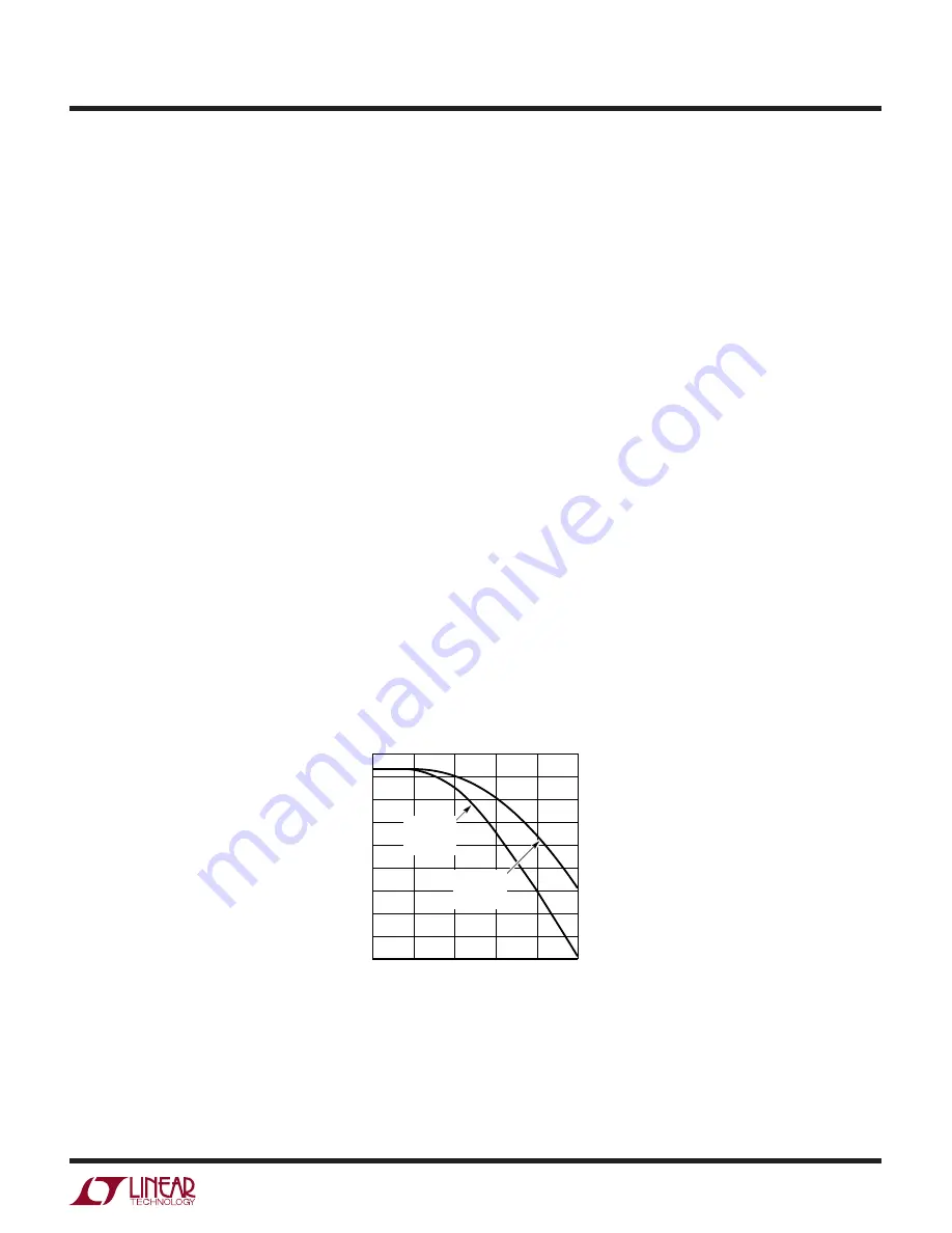
Figure 4. Maximum Inductor Peak Current Vs Duty Cycle
DUTY CYCLE (%)
0
MAXIMUM INDUCTOR PEAK CURRENT (mA)
950
900
850
800
750
700
650
600
550
500
80
DC257 F04
20
40
60
100
WITH
EXTERNAL
CLOCK
WITHOUT
EXTERNAL
CLOCK
UNDERVOLTAGE LOCKOUT
A precision undervoltage lockout shuts down the LTC1707
when V
IN
drops below 2.7V, making it ideal for single
lithium-ion battery applications. In shutdown, the LTC1707
draws only several microamperes, which is low enough to
prevent deep discharge and possible damage to a lithium-
ion battery nearing its end of charge. A 150mV hysteresis
ensures reliable operation with noisy supplies.
LOW SUPPLY OPERATION
The LTC1707 is designed to operate from supply voltages as
low as 2.85V. At this voltage, the converter is most likely to
be running at high duty cycles or in dropout, where the main
switch is on continuously. Hence, the I
2
R loss is due mainly
to the R
DS(ON)
of the P-channel MOSFET. See the LTC1707
data sheet for additional information.
SLOPE COMPENSATION AND
PEAK INDUCTOR CURRENT
Slope compensation provides stability by preventing sub-
harmonic oscillations. It works by internally adding a ramp
to the inductor current signal at duty cycles in excess of
40%. As a result, the maximum inductor peak current is
lower for V
OUT
/V
IN
> 0.4 than when V
OUT
/V
IN
< 0.4. See the
maximum inductor peak current vs duty cycle graph in
Figure 4.
The graph labeled “With External Clock” shows the worst-
case peak current reduction obtained when the oscillator
is synchronized at its minimum frequency, that is, to a
clock just above the oscillator’s free-running frequency.
HOW TO MEASURE VOLTAGE REGULATION
When trying to measure voltage regulation, remember
that all measurements must be taken at the point of
regulation. This point is where the LTC1707’s control loop
looks for the information to keep the output voltage
constant. In this demonstration board, this information
point occurs between Pin 4, the GND of the LTC1707, and
the output side of R7. These points correspond to the GND
(E5) and V
OSENSE
(E6) terminals of the board. Output
voltage test leads should be attached directly to these
terminals. The load should be placed between V
OUT
(E7)
and GND (E5). Measurements
should not be taken at the
end of test leads at the load. Refer to Figure 5 for the proper
monitoring equipment configuration.