background image

2

dc1721bf

DEMO MANUAL 
DC1721B-A/DC1721B-B

 QUICK START PROCEDURE

Demonstration circuit 1721 is easy to set up to evaluate the 
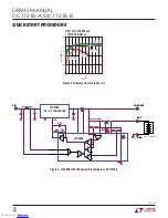
performance of the LTC4000/LTC3789. Refer to Figure 1 
for proper measurement equipment setup and follow the 
procedure below:

WARNING: BATTERIES ARE POTENTIALLY DANGER-
OUS HIGH ENERGY SOURCES. IMPROPER CON-
NECTION, OVERCHARGE, OR RAPID DISCHARGE 
COULD RESULT IN EXPLOSION AND/OR FIRE.

NOTE. When measuring the output voltage ripple, care must 
be taken to avoid a long ground lead on the oscilloscope 
probe. Measure the output voltage ripple by touching the 
probe tip and ground ring directly across the last output 
capacitor as shown in Figure 1.

1.  Set MODE jumper to CCM. Set CHARGE jumper to 

DISABLE.

2.  Set an input power supply that is capable of 6V to 36V 

and 12A to 24V. Then turn off the supply.

3.  With power off, connect the supply to the input terminals 

VIN and GND.

NOTE.

a.  Input voltages lower than 6V can keep the converter 

from turning on due to the undervoltage lockout feature 
of the LTC4000.

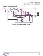
b.  If efficiency measurements are desired, refer to Figure 1 

for test setup.

4.  Turn on the power at the input.

NOTE. Make sure that the input voltage never exceeds 36V.

5.  Check for the proper VOUT-SYS of 15.3V. Turn off the 

power at the input.

6.  Once the proper output voltages are established, con-

nect a variable load capable of sinking 7A at 16V to the 
output terminals VOUT-SYS and GND. Set the current 
for 0A.

7.  Turn on the power at the input.

NOTE. If there is no output, temporarily disconnect the 
load to make sure that the load is not set too high.

8.  Once the proper VOUT-SYS is again established, adjust 

the load and/or source within the operating range and 
observe the output voltage regulation, ripple voltage, 
efficiency, input and output current limit, and other 
desired parameters.

9.  Turn off the power at the input.

10. Connect the output load and meters to the BAT output.

11. Set CHARGE jumper to ENABLE.

12. Turn on the power at the input.

13. Once the proper VOUT-SYS is again established, adjust 

the load and/or source within the operating range and 
observe the battery float voltage regulation and other 
desired parameters.

14. Set the load to constant voltage mode to more easily 

observe charge current and trickle charge current.

15. 

(DC1721B-B 0NLY)

 In order to observe MPP operation, 

add a 0.25Ω to 0.3Ω, 10W resistor in series with the 
DC source and set the source to 13V. Use a constant 
voltage or constant resistance load characteristic. As 
the load is increased, the input voltage will be regulated 
at the MPP regulation point (11.75V) by reducing the 
output of the DC/DC converter.

NOTE. Operation in the Instant-On region (V

OUT

 < 12.5V) 

may engage thermal limit circuit to protect Q7 in the linear 
region.

NOTE. The optional thermal limit circuit for Q6 (Q9, RNTC3, 
R55-59, and U4) is included to protect Q6 in case of an 
extended short circuit on VOUT-SYS under adverse thermal 
conditions (T

A

 > 40°C). It may not be needed in applica-

tions with less severe thermal conditions, lower current 
available to VOUT-SYS, or where continuous short-circuit 
protection on VOUT-SYS is not required.

Downloaded from

Arrow.com.

Downloaded from

Arrow.com.

Содержание DC1721B-A

Страница 1: ...portableapplicationsincludinginstruments industrial equipment power tools and computers It has a total footprint area of 12 4cm2 3 6cm2 for the LTC4000 circuit only Synchronous rectification helps to attain efficiency exceeding 96 at full load and nominal input DC1721B A The LTC4000 has an input current limit regulation loop that prevents overloading sources with limited output capability DC1721B ...

Страница 2: ...s no output temporarily disconnect the load to make sure that the load is not set too high 8 OncetheproperVOUT SYSisagainestablished adjust the load and or source within the operating range and observe the output voltage regulation ripple voltage efficiency input and output current limit and other desired parameters 9 Turn off the power at the input 10 Connect the output load and meters to the BAT...

Страница 3: ...EMO MANUAL DC1721B A DC1721B B QUICK START PROCEDURE Figure 1 Proper Measurement Equipment Setup Figure 2 Proper Noise Measurement Setup Downloaded from Arrow com Downloaded from Arrow com Downloaded from Arrow com ...

Страница 4: ... LTC4000 Gm Gm Gm Gm LTC3789 NOT ON THE BOARD GND GND RC1 RC1 CC1 CC1 VOUT SYS VOUT SYS BAT BAT VIN VIN 10nF 10nF CC2 CC2 Figure 3 Efficiency from VIN to VOUT SYS DC1721A LTC4000 and LTC3789 Efficiency IOUT A 0 5 EFFICIENCY 100 95 85 90 80 2 5 4 5 1 5 3 5 5 5 VIN 36V VIN 24V VIN 6V VIN 15V Downloaded from Arrow com Downloaded from Arrow com Downloaded from Arrow com Downloaded from Arrow com ...

Страница 5: ...A10 A8 A9 Rsense charge DC DC CONVERTER ITH LTC4000 1 Gm Gm Gm Gm LTC3789 NOT ON THE BOARD GND GND RC1 RC1 CC1 CC1 VOUT SYS VOUT SYS BAT BAT VIN VIN 10nF 10nF CC2 CC2 QUICK START PROCEDURE Downloaded from Arrow com Downloaded from Arrow com Downloaded from Arrow com Downloaded from Arrow com Downloaded from Arrow com ...

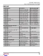
Страница 6: ...KY 40V 2A SMA DIODES ZETEX B240A 13 F 21 1 D9 DIODE ZENER 3V 500MW SOD 323 DIODES ZETEX BZT52C3V0S 7 F 22 1 F1 FUSE 6 3A 32V T LAG 1206 SMD COOPER BUSSMAN 3216TD6 3 R 23 1 L1 INDUCTOR 4 7μH TOKO FDA1254 4R7M 24 2 Q2 Q4 MOSFET N Chan 40V POWERPAK 8 VISHAY SiR422DP T1 GE3 25 2 Q3 Q5 MOSFET N Chan 20V POWERPAK 8 VISHAY SiR496DP T1 GE3 26 2 Q6 Q7 MOSFET P Chan 30V POWERPAK 8 VISHAY Si7135DP T1 GE3 27 ...

Страница 7: ...al Demo Board Circuit Components 57 0 C3 C23 C26 C27 OPT 1210 58 1 C33 CAP X5R 4 7μF 10V 20 0603 AVX 0603ZD475MAT2A 59 1 CBAT CAP X5R 2 2μF 25V 20 0805 AVX 08053D225MAT2A 60 0 CF1 CC1 R6 C7 C8 C11 R12 R22 R27 R30 R38 R43 R53 R61 R62 CNTC CF CCX OPT 0603 OPT 61 2 CIIMON CIBMON CAP C0G 1000pF 25V 5 0603 AVX 06033A102JAT2A 62 0 CIN3 CIN4 OPT 63 0 D11 OPT SOD323 OPT 64 1 LED2 LED DUAL RED GREEN LiteOn...

Страница 8: ...C3V0S 7 F 21 1 D10 DIODE ZENER 5 6V 500MW SOD 123 DIODES ZETEX BZT52C5V6 7 F 22 1 F1 FUSE 6 3A 32V T LAG 1206 SMD COOPER BUSSMAN 3216TD6 3 R 23 1 L1 INDUCTOR 4 7μH TOKO FDA1254 4R7M 24 2 Q2 Q4 MOSFET N Chan 40V POWERPAK 8 VISHAY SiR422DP T1 GE3 25 2 Q3 Q5 MOSFET N Chan 20V POWERPAK 8 VISHAY SiR496DP T1 GE3 26 2 Q6 Q7 MOSFET P Chan 30V POWERPAK 8 VISHAY Si7135DP T1 GE3 27 2 Q8 Q9 MOSFET SMALL SIGNA...

Страница 9: ... DC1721B B Additional Demo Board Circuit Components 58 0 C3 C23 C26 C27 OPT 1210 59 1 C33 CAP X5R 4 7μF 10V 20 0603 AVX 0603ZD475MAT2A 60 1 CBAT CAP X5R 2 2μF 25V 20 0805 AVX 08053D225MAT2A 61 0 CF1 CC1 R6 C7 C8 C11 R12 R22 R27 R30 R38 R43 R53 R61 R62 CNTC CF CCX OPT 0603 OPT 62 2 CIIMON CIBMON CAP C0G 1000pF 25V 5 0603 AVX 06033A102JAT2A 63 0 CIN3 CIN4 OPT 64 0 D11 OPT SOD323 OPT 65 1 LED2 LED DU...

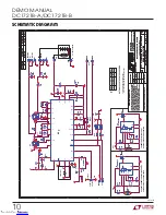
Страница 10: ...HOWEVER IT REMAINS THE CUSTOMER S RESPONSIBILITY TO VERIFY PROPER AND RELIABLE OPERATION IN THE ACTUAL APPLICATION COMPONENT SUBSTITUTION AND PRINTED CIRCUIT BOARD LAYOUT MAY SIGNIFICANTLY AFFECT CIRCUIT PERFORMANCE OR RELIABILITY CONTACT LINEAR TECHNOLOGY APPLICATIONS ENGINEERING FOR ASSISTANCE THIS CIRCUIT IS PROPRIETARY TO LINEAR TECHNOLOGY AND SCHEMATIC SUPPLIED FOR USE WITH LINEAR TECHNOLOGY ...

Страница 11: ...ONS HOWEVER IT REMAINS THE CUSTOMER S RESPONSIBILITY TO VERIFY PROPER AND RELIABLE OPERATION IN THE ACTUAL APPLICATION COMPONENT SUBSTITUTION AND PRINTED CIRCUIT BOARD LAYOUT MAY SIGNIFICANTLY AFFECT CIRCUIT PERFORMANCE OR RELIABILITY CONTACT LINEAR TECHNOLOGY APPLICATIONS ENGINEERING FOR ASSISTANCE THIS CIRCUIT IS PROPRIETARY TO LINEAR TECHNOLOGY AND SCHEMATIC SUPPLIED FOR USE WITH LINEAR TECHNOL...

Страница 12: ...E OTHER FOR ANY INDIRECT SPECIAL INCIDENTAL OR CONSEQUENTIAL DAMAGES The user assumes all responsibility and liability for proper and safe handling of the goods Further the user releases LTC from all claims arising from the handling or use of the goods Due to the open construction of the product it is the user s responsibility to take any and all appropriate precautions with regard to electrostati...

Отзывы: