background image

9

dc1605bf

DEMO MANUAL DC1605B

Quick start proceDure

4. Launch the LTpowerPlay GUI.
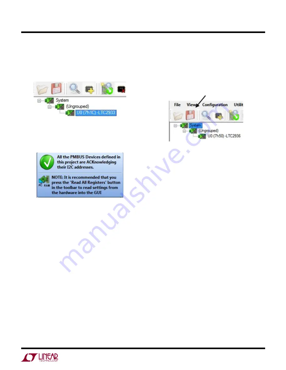
  a. The GUI automatically identifies the DC1605B and 

builds a system tree for each I

2

C device. The system 

tree on the left hand side will look like this: 

  b. A green message box will be displayed momentarily 

in  the  lower  left  hand  corner  confirming  that  the 

DC1605B is communicating. The board at this point 

is fully operational.

5. Load the Demo Configuration.

In the upper left hand corner of the GUI, select File > 

Initialize DC1605B Demo > Demo Config (or Factory 

Defaults). This will load the configuration settings into 

the working RAM of the LTC2936, set the DAC outputs, 

clear the status registers, and store the settings into 

NVM (EEPROM). The ‘Demo Config’ file is the starting 

point for the use cases. The ‘Factory Defaults’ file sets 

the V

n

 thresholds that accommodate the initial powerup 

state of the DAC outputs (2.048V).

SAVING A CONFIGURATION

You can make changes to the LTC2936 register values 

and DAC settings. Save the demo board configuration to 

a (*.proj) file by clicking the "Save" icon. This creates a 

backup file. Name it whatever you like. Note that the DAC 

settings are saved in the project file. 

QUICk START VIDEO

There is a Quick Start Video that covers the basic features 

of the LTC2936 chip and DC1605B demo board. The video 

can be accessed via LTpowerPlay by navigating to the Help 

menu > DC1605B Content.

LOADING A DC1605B CONFIGURATION (*.proj) FILE 

WITH THE GUI

1. In the upper left hand corner of the GUI, File > Open 

> browse to your *.proj file. This will load the file into 

the GUI.

2. Click on the “Go Online” icon, then click on the “PC 


RAM” icon to write all registers. This loads the configu-

ration into the working RAM of the LTC2936. The DAC 

settings are stored and retrieved from the .proj file.

3. To store the configuration to NVM (EEPROM), click on 

the “RAM 

→ 

NVM” icon

Содержание DC1605B

Страница 1: ...2936 The board comes pre programmed with the EEPROM values appropriate for the six power supply rails on the DC1605B Just plug and play The LTC2936 chip is mounted on the topside of the board with support ADC and DAC circuitry on the back The ADC provides voltage readings for all six voltage supervisor inputs on the LTC2936 and also reads the GPI and GPIO voltages The DAC drives six programmable v...

Страница 2: ...unction and map behavior to a GPIO pin Nominal VTH 0 5V EEPROM Non volatile memory NVM storage used to retain data after power is removed Margin Term used typically in board level testing that increases decreases the output voltage to look for sensi tivity marginality problems MARG Ignoremargining OVandUV whenactive low A GPI pin may be programmed to this function and map behavior to a GPIO pin No...

Страница 3: ... programs each voltage supervi sor srange polarity mapping andhighandlowthreshold voltages Each channel s high low comparators may be mapped to any GPIO pin and any comparator may be mapped to multiple GPIO pins Typically the high comparator is used for the overvoltage condition and the low comparator is usedfortheundervoltagecondition Thehighcomparatoris notdedicatedastheOVdetectionnoristhelowcom...

Страница 4: ...board via the DC1613 USB controller The controller provides 5V supply and I2C SMBus read write control This setup provides an easy quick way to demonstrate the LTC2936 s capabilities GPIO INPUT OPTIONS MANUAL RESET MARGIN UV DISABLE AUXC NO PULL UP INTERNAL LOGIC LTC2936 6 CH VOLTAGE SUPERVISOR WITH EEPROM V1 V2 V3 V4 V5 V6 VPWR GPIO1 GPIO2 GPIO3 GPI1 GPI2 BLUE RED BLUE RED BLUE RED GREEN 3 3VOUT ...

Страница 5: ... replicate the user s system rails This avoids the need for the user to wire actual supply rails to the demo board however the board was designed to allow this use case The DAC output range is 0V to 4V This is sufficient for demo purposes Simply place the V1 V6 jumpers to INT for internal DAC use and ensure the LTC2936 is powered by setting JP9 appropriately Powering the Board The DC1605B board ca...

Страница 6: ...2936 will be grayed out in the system tree DC1605B ToolWindow and GUI Indicators TheToolWindowdisplaystheADCreadingsontheleftand DAC voltage settings on the right The blue red indicators next to the GPIs and GPIOs display the state H vs L and voltage reading from the ADC LT2499 Blue indicates a logic high and red indicates a logic low The ToolWindow is automatically populated when LTpowerPlay dete...

Страница 7: ...des unprec edented system level diagnostic and debug features It becomesavaluablediagnostictoolduringboardbring up to program or tweak the power management scheme in a system or to diagnose power issues when bringing up rails LTpowerPlayutilizestheDC1613I2C SMBus PMBus controller to communicate with one of many potential tar gets including the DC1605B demo system or a customer board The software a...

Страница 8: ... protective bag and place it on a level surface Connect the DC1613 I2C SMBus PMBus controller to the DC1605B board using the 12 pin ribbon cable 3 Plug the USB to I2C SMBus PMBus Controller into a USB port on your PC The board should power up with 5V and 3 3VOUT LEDs illuminated green The GPIO and CMP LEDs will illuminate blue Figure 4 Connecting DC1605B Board and the DC1613 USB to I2C SMBus PMBus...

Страница 9: ... theVnthresholdsthataccommodatetheinitialpowerup state of the DAC outputs 2 048V Saving a Configuration You can make changes to the LTC2936 register values and DAC settings Save the demo board configuration to a proj file by clicking the Save icon This creates a backup file Name it whatever you like Note that the DAC settings are saved in the project file Quick Start Video There is a Quick Start V...

Страница 10: ...ration REFERENCE DESIGNATOR SIGNAL NAME USAGE DEFAULT JP1 JP6 V1 V6 Selects internal vs external voltage INT JP7 JP8 ASEL1 ASEL0 Selects H Z L for LTC2936 slave address L JP9 VPWR Selects internal 5V external 3 3V or remove to apply 3 4V to 14V turret INT Figure 5 DC1605B Top Side Details ...

Страница 11: ... and activated when the pushbutton switches are depressed GPIO1 OV fault GPIO2 ALERT latched GPIO3 UV fault GPI1 MR manual reset GPI2 MARG ignore OV UV when margining Let s margin V5 and V6 low by typing a value of 1V and 0 9V into the respective DAC control boxes You may also move the DAC output by clicking the up down arrows on theindividualDACboxorbydouble clickingtheDACvalue and entering a new...

Страница 12: ...ent is 700µA For example a 5V external supply may be connected to turretV1 NoticetheGPIO1andGPIO2LEDsturnred indi cating OV and ALERT are asserted low The V2 thresholds need to be changed Enter 5 5V and 4 5V for the HI and LO thresholdsettings TheGPIO1willreturnhighandtheLED will change to blue but the GPIO2 remains low red since it indicates a latched ALERT Press the MR pushbutton on GPI1 to rele...

Страница 13: ...PI1asaManualReset MapGPI1toGPIO1 3 Configure GPIO1 as active low with weak pull up To update the changes made in steps 1 3 click the Write All Registers PC RAM icon 4 You can optionally extend the low time of the system resetbychangingthedelay on releasesettingtoensure a clean release of reset This provides a time based debounce of the switch Whenconfiguredinthisway GPIO1providesasystemreset for t...

Страница 14: ... POINT TURRETS FOR V1 V6 TEST POINT TURRETS FOR GPO1 3 V1 V6 JUMPERS I2 C TURRETS TO DC1613 6V TO 14V POWER JACK TURRET AND LED INDICATING 5V POWER FOR DC1605B CMP1 6 HEADER TEST POINT TURRETS FOR GPI1 2 SIGNALS GPI PUSHBUTTON SWITCHES SLAVE ADDRESS JUMPERS ...

Страница 15: ...15 dc1605bf DEMO MANUAL DC1605B DC1605B Details Bottom ...

Страница 16: ... 1W 1 0603 SMD VISHAY CRCW0603604KFKEA 17 6 R22 R23 R24 R62 R64 R66 RES 100k 0 1W 1 0603 SMD VISHAY CRCW0603100KFKEA 18 0 R31 R32 R33 R49 R51 R53 OPTIONAL RES 0Ω 0 1W 1 0603 SMD 19 8 R34 R35 R36 R37 R38 R50 R52 R54 RES 0Ω 0 1W 1 0603 SMD VISHAY CRCW060366K5FKEA 20 2 R39 R40 0Ω RESISTOR ARRAY 4 RES 1206 PANASONIC EXB 38VR000V 21 1 R43 RES 49 9k 0 1W 1 0603 SMD VISHAY CRCW060349K9FKEA 22 1 R45 RES 2...

Страница 17: ...17 dc1605bf DEMO MANUAL DC1605B Schematic Diagram ...

Страница 18: ...18 dc1605bf DEMO MANUAL DC1605B Schematic Diagram ...

Страница 19: ...logy Corporation is believed to be accurate and reliable However noresponsibilityisassumedforitsuse LinearTechnologyCorporationmakesnorepresenta tion that the interconnection of its circuits as described herein will not infringe on existing patent rights Schematic Diagram ...

Страница 20: ...UDING ANY WARRANTY OF MERCHANTABILITY OR FITNESS FOR ANY PARTICULAR PURPOSE EXCEPT TO THE EXTENT OF THIS INDEMNITY NEITHER PARTY SHALL BE LIABLE TO THE OTHER FOR ANY INDIRECT SPECIAL INCIDENTAL OR CONSEQUENTIAL DAMAGES The user assumes all responsibility and liability for proper and safe handling of the goods Further the user releases LTC from all claims arising from the handling or use of the goo...

Отзывы: