


- 30/132-
LG Electronics Inc.
1.2.6 RFR6500 - Down-converter Mixers part (U105)
all the circuitry (with the exception of external filters) needed to support conversion of received RF signals to Base-
band signals. The three down-converting Mixers (Cellular, PCS and GPS), and a programmable PLL for generating
RX LO frequency and an RX LO Buffer Amplifier and RX Voltage Controlled Oscillator. The GPS LNA & mixers
offer the most advanced and integrated CDMA RX solution designed to meet cascaded Noise Figure (NF) and Third-
order Intercept Point (IIP3) requirements of IS-98D and J-STD-018 specifications for Sensitivity, Two-Tone Inter-
modulation, and Single-tone Desensitization.
Operation modes and band selection are specially controlled from the Mobile Station Modem
MSM6550A.
The specification of VX9700 Mixers is described below:
Low gain
High gain
Units
Cellular
PCS
Cellular
PCS
Noise Figure
25
27
7.9
12
dB
Input IP3
-5
-11
4
4
dBm
Input IP2
30
30
56
56
dBm
Parameter
1.3 Description of Transmit Part Circuit
1.3.1 RFT6150 (U102)
The RFT6150 Base-band to RF Transmit Processor performs all TX signal-processing functions required between
digital Base-band and the Power Amplifier Modulator (PAM). The Base-band quadrate signals are up-converted to
the Cellular or PCS frequency bands and amplified to provide signal drive capability to the PAM. The RFT6150
includes mixers for up-converting analog Base-band to RF, a programmable PLL for generating TX LO frequency a
TX LO Buffer Amplifier and TX Voltage Controlled Oscillator, cellular and PCS driver amplifiers and TX power
control through an 85 dB VGA. As added benefit, the single sideband up-conversion eliminates the need for a band
pass filter normally required between the up-converter and driver amplifier.
I, I/, Q and Q/ signals proceed from the MSM6550A to RFT6150 are analog signal. In CDMA mode, These signals
are modulated by Offset Quadrature Phase Shift King (OQPSK). I and Q are 90 deg. out of phase, and I and I/ are
180 deg. The mixers in RFT6150 converts baseband signals into RF signals. After passing through the upconverters,
RF signal is inputted into the Power AMP.
Z3X-BOX.COM
Содержание VX9700
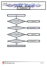
Страница 26: ... 25 132 LG Electronics Inc VX9700 28 Powering Down Restart Z 3 X B O X C O M ...
Страница 47: ... 46 132 LG Electronics Inc VX9700 Waveform Waveform 4 1 1 e 4 1 1 f F106 pin2 DP1 pin3 Z 3 X B O X C O M ...
Страница 59: ... 58 132 LG Electronics Inc VX9700 Waveform Waveform F106 pin2 DP2 pin2 Z 3 X B O X C O M ...
Страница 93: ... 92 132 LG Electronics Inc VX9700 Test point Test point DSP_CLK C601 DSP_CLK Z 3 X B O X C O M ...
Страница 105: ... 104 132 LG Electronics Inc VX9700 Test point Test point C519 U408 U502 U501 R552 C515 C514 R551 Z 3 X B O X C O M ...
Страница 111: ... 110 132 LG Electronics Inc VX9700 Test point Test point C202 C203 U50 1 C20 05 U3004 L802 L801 Z 3 X B O X C O M ...
Страница 139: ... 2 132 LG Electronics Inc VX9700 2 132 LG Electronics Inc VX9700 Appendix 2 Block and Circuit Diagram Z 3 X B O X C O M ...
Страница 154: ...CON104 Z 3 X B O X C O M ...
Страница 156: ...Z 3 X B O X C O M ...
Страница 157: ...SPCY0126601_1 0 RCV MOT VX9700_F_SUB R 8 2 4 C O N 8 1 0 U 8 0 1 U 8 0 2 U 8 0 3 U 8 0 4 U 8 0 5 Z 3 X B O X C O M ...
Страница 159: ...CON809 SW101 SW102 Z 3 X B O X C O M ...
Страница 160: ...CON808 Z 3 X B O X C O M ...
Страница 162: ...CON809 SW104 Z 3 X B O X C O M ...
Страница 163: ...CON808 Z 3 X B O X C O M ...
Страница 165: ...SW1 CON2 Z 3 X B O X C O M ...
Страница 166: ...CON1 Z 3 X B O X C O M ...
Страница 167: ... 15 132 LG Electronics Inc VX9700 Appendix 3 Part List VX9700 Part List Z 3 X B O X C O M ...
Страница 168: ... 16 132 LG Electronics Inc VX9700 Appendix 4 Components Layout Z 3 X B O X C O M ...
Страница 170: ... 18 132 LG Electronics Inc VX9700 ANT301 BT ANTENNA ACS2450HCCVX97 No BT Communication Z 3 X B O X C O M ...
Страница 173: ... 21 132 LG Electronics Inc VX9700 CAMERA KEY FPCB SW104 CAMERA KEY LS51D 23T Z 3 X B O X C O M ...
Страница 174: ...Z 3 X B O X C O M ...


