background image

LG-

U

D6100 


LGE


LG Electronics Inc.

     15/21 

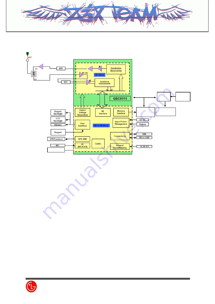
[Figure 3-1] Block Diagram Of RD6100 


Camera 

IC

LCD

(128*128CSTN)

Camera 

(VGA)

FM Radio

MCP

64*32Mb


1.2 Description of Receive Part Circuit 


1.2.1 Duplexer (DP101)


The duplexer consists of the receive part bandpass filter (BPF) and the transmit part bandpass filter 

(BPF) which have the function of separating transmit/receive signals in the full duplex system using 

the transmit/receive common antenna. The transmit part BPF is used to suppress noises and spurious 

waves entering the receive band among transmit signals in order to prevent the drop in receive 

sensitivity characteristics. The receive part BPF blocks the signals sent out from entering the receive 

end in order to improve sensitivity characteristics. 

Insertion loss (IL) in the transmit band is 2.8dB (Max), whereas IL in the receive band is 3.5dB (Max). 

The receive band attenuation amount of transmit filter is 45dB (Min) and the transmit band attenuation 

amount of receive filter is 57dB or more (Min).


Z3X-BOX.COM

Содержание LG-UD6100

Страница 1: ... board channel 5 Voltage and Current Value of Termination Part Amplifier Catalogue included Mode Type Name Voltage Current Power CDMA SKY77162 3 4V 455mA 0 282W 6 Functions of Major Semi Conductors Classification Function QSC6010 MSM baseband radioOne RF and power management MCP PF38F2040W0YBQE Flash Memory 64Mbit Storing of the mobile station operation program MCP PF38F2040W0YBQE PSRAM 32Mbit Tem...

Страница 2: ...CDMA MOBILE SUBSCRIBER UNIT LG UD6100 SINGLE BAND CDMA MOBILE PHONE SERVICE MANUAL Z 3 X B O X C O M ...

Страница 3: ... CDMA Mobile Phone 5 3 Structure and Functions of CDMA Mobile Phone 8 4 Specification 9 5 Installation 12 Chapter 2 NAM Input Method 13 Chapter 3 Circuit Description 14 1 RF Transmit Receive Part 14 2 Digital Voice Processing Part 18 Chapter 4 Trouble Shooting 22 Block Diagram 56 Circuit Diagram 57 PCB Layout 62 Exploded View 64 Part List 67 Z 3 X B O X C O M ...

Страница 4: ...ombined into this phone to reduce the call being interrupted in a middle of talking over phone CDMA digital cellular network consists of MSC Mobile Switching Office BSC Base Station Controller BTS Base station Transmission System and MS Mobile Station Communication between MS and BTS is designed to meet the specification of TIA EIA IS 95 A B C Common Air Interface MS meets the specifications of th...

Страница 5: ...nce The analog cellular systems are classified further into an AMPS system E AMPS System NMT system ETACS system and JTACS system depending on technologies used Unlike the Time Division Multiple Access TDMA or the Frequency Division Multiple Access FDMA used in the band limited environment the Code Division Multiple Access CDMA system which is one of digital cellular systems is a multi access tech...

Страница 6: ...everal CDMA signals are overlapped Among these types of signals only desired signal energy is selected and received through the use of pre determined binary sequence desired signals can be separated and then received with the correlator used for recovering the spectrum into its original state At this time the spectrums of other signals that have different codes are not recovered into its original ...

Страница 7: ...e station to mobile stations and backward from the mobile station to the base station power control in order to increase the call processing capacity and obtain high quality calls In case the originating signals of mobile stations are received by the cell site in the minimum call quality level signal to interference through the use of transmit power control on all the mobile stations the system ca...

Страница 8: ...ted for use depending on inputted automatic conditions and message data both of them utilize four stage frames of 9600 4800 2400 and 1200 bits per second In addition this type of variable voice encoder utilizes adaptive threshold values when selecting required data rate It is adjusted in accordance with the size of background noise and the data rate is increased to high rate only when the voice of...

Страница 9: ...ell site about 65 In the case of directional cell site one cell normally uses a 120 sector antenna in order to divide the sector into three In this case each antenna is used only for 1 3 of mobile stations in the cell site and accordingly interference is reduced by 1 3 on the average and the capacity that can be supported by the entire system is increased by three times 2 7 Soft Capacity The subsc...

Страница 10: ...During the operation with one cell site the searcher searches out multi paths in accordance with terrain and building reflections On three data receivers the most powerful four paths are allocated for the parallel tracing and receiving Fading resistance can be improved a great deal by obtaining the diversity combined output for de modulation Moreover the searcher can be used to determine the most ...

Страница 11: ...mperature 30 60 4 1 6 Frequency Stability 0 5PPM 4 1 7 Antenna Fixed PIFA Type Internal 50 Ω 4 1 8 Size and Weight Size 104 x 46 x 13 9mm L x W x D Weight 73g 4 1 9 Channel Spacing 1 25MHz 4 1 10 Battery Type Capacity and Orerating Time Unit Hours Minutes Standard 950mAh Stand By Time 140 Hrs SCI 2 Talk Time 145 Min Cell power 92dBm 4 2 Receive Specification 4 2 1 Frequency Range 869 820 MHz 893 1...

Страница 12: ...the 1 23MHz band 4 3 Transmit Specification 4 3 1 Frequency Range 824 820 MHz 848 190 MHz 4 3 2 Intermediate Frequency QSC60X0 seires Zero IF 4 3 3 Output Power 0 251W 4 3 4 Interference Rejection Single Tone 30dBm at 900 kHz Two Tone 43dBm at 900 kHz 1700kHz 4 3 5 CDMA TX Frequency Deviation 300Hz or less 4 3 6 CDMA TX Conducted Spurious Emissions 900kHz 42 dBc 30kHz below 1 98MHz 54 dBc 30kHz be...

Страница 13: ...80 MHz 840 810 MHz 842 04 MHz 843 270 MHz 844 500 MHz 845 910 MHz 847 140 MHz 848 370 MHz 4 5 MS Mobile Station Receiver Frequency FA NO CH NO CENTER FREQUENCY FA NO CH NO CENTER FREQUENCY 1 2 3 4 5 6 7 8 9 10 1011 29 70 111 152 193 234 275 316 363 869 640 MHz 870 870 MHz 872 100 MHz 873 330 MHz 874 560 MHz 875 790 MHz 877 020 MHz 878 250 MHz 879 480 MHz 880 890 MHz 11 12 13 14 15 16 17 18 19 20 4...

Страница 14: ...y is being charged Green light indicates battry is fully charged 5 3 For Mobile Mount 5 3 1 Installation Position In order to reduce echo sound when using the Hands Free Kit make sure that the speaker and microphone are not facing each other and keep microphone a generous distance from the speaker 5 3 2 Cable Connections 5 3 2 1 Power and Ignition Cables Connect the red wire to the car battery pos...

Страница 15: ...ve To reset the handset press END CHAPTER 2 NAM Input Method Inputting of MIN included 2 NAM Input Method Inputting of telephone numbers included 1 ESN 2 MIN 3 NAM Name 4 Security Code 5 MCC 6 NMSID 7 IMSI_T MCC 8 IMSI_T NMSID 9 PRL Enabled 10 MDN 11 CDMA Home SID 12 CDMA Home NID 1 HOW TO POWER UP 13 CDMA Pri ChA 14 CDMA Sec ChA 15 CDMA Pri ChB 16 CDMA Sec ChB 17 Lockout SID 18 Lockout NID 19 Hom...

Страница 16: ...ly Baseband signals created are changed into digital signals by the analog digital converter ADC A D Converter and then auto gain controlled and are demodulated by the modulator demodulator In the case of transmission QSC6010 modulates interpolates and converts the digital signal into an analog baseband before upconverts the Tx analog baseband into RF The baseband quadrature signals are upconverte...

Страница 17: ...nsmit receive common antenna The transmit part BPF is used to suppress noises and spurious waves entering the receive band among transmit signals in order to prevent the drop in receive sensitivity characteristics The receive part BPF blocks the signals sent out from entering the receive end in order to improve sensitivity characteristics Insertion loss IL in the transmit band is 2 8dB Max whereas...

Страница 18: ...s and converts the digital signal into an analog baseband and upconverts the Tx analog baseband into RF The QSC6010 communicates with the external RF and analog baseband to control signal gain in the RF Rx and Tx signal paths educe base band offset errors and tune the system frequency reference The QSC6010 baseband to RF Transmit Processor performs all Tx signal processing functions required betwe...

Страница 19: ...uit are integrated onto one IC after going through the GaAs HBT heterojunction bipolar transistor process The module of power amplifier is made up of an output end interface circuit including this module The maximum power that can be inputted through the input terminal is 8dBm and conversion gain is about 28 5dB RF transmit signals that have been amplified through the power amplifier are sent to t...

Страница 20: ...d a receptacle that receives and sends out voice and data with external sources 2 2 2 Voice Processing Part The voice processing part is made up of an audio codec in QSC6010 used to convert MIC signals into digital voice signals and other external MIDI Synthesizer used to convert digital voice signals into analog voice signals amplifying parts for amplifying the voice signals and MIC signals are o...

Страница 21: ...6030 device only and MIDI and MP3 functions are supported by the various QSC tiers as indicated in Table 1 2 The baseband function reduces part costs by using two external bus interfaces to support next generation memory architectures such as NAND FLASH SRAM and pseudo SRAM PSRAM page and burst mode NOR or MLC NOR FLASH The EBI2 also serves as an enhanced LCD interface A variety of connectivity op...

Страница 22: ...the ear piece 2 3 3 Memory Part The memory part consists of a 32Mbits Flash Memory and a 16Mbits SRAM On the Flash Memory there are programs used for the operation of a mobile station and the non volatile data of the mobile station such as a ESN Electronic Serial Number are stored The programs can be changed through down loading after the assembling of mobile stations On the SRAM data generated du...

Страница 23: ...32 bit internal data bus It has a high performance and low power consumption FLASH ROM and SRAM Flash Memory is used to store the program of the mobile station Using the down loading program the program can be changed even after the mobile station is fully assembled SRAM is used to store the internal flag information call processing data and timer data KEYPAD For key recognition key matrix is setu...

Страница 24: ...When Rx Sensitivity isn t good enough Test Point 4 1 Rx Part Trouble CHAPTER 4 Trouble Shooting CHAPTER 4 Trouble Shooting QSC6010 Duplexer Z 3 X B O X C O M ...

Страница 25: ...Circuit Diagram Z 3 X B O X C O M ...

Страница 26: ...p CH 610 1 Check RF cable Loss 2 Check RF path Circuit connection 3 Check U101 DP101 F102 Checking Flow NG Change RF cable or re set loss NG Re work or replace them NG Replace them Download S W Calibrate Replace QSC6010 or main board NG Z 3 X B O X C O M ...

Страница 27: ...7 then click offline d Click Band select to cdma Tx on Power Amp On Set channel to 610 AGC 400 Spectrum analyzer setting Oscilloscope setting 1 Check PAM Circuit 2 Check Duplexer Mobile SW Circuit 3 Check QSC6010 circuit Redownload SW CAL Duplexer PAM Mobile S W QSC6010 TX filter Z 3 X B O X C O M ...

Страница 28: ...4 2 1 Check PAM Circuit Test Point Circuit Diagram U103 Pin7 RF_OUT U103 Pin 1 8 Vcc1 2 U103 Pin2 RF_IN U103 Pin4 Vref 2 85V Z 3 X B O X C O M ...

Страница 29: ...RF_IN YES Check U103 Pin4 V_ref Check F101 circuit Check Q101 circuit NO Level is 3 2V 4 2V OK YES Check U103 Pin1 8 VCC1 2 Check C206 U201 NO Output Level is Appear YES Check U103 Pin7 RF_OUT Replace U103 Waveform U103 Pin2 DCN PAM_IN U103 Pin7 DCN PAM_OUT SPECTRUM ANALYZER CONDITION RBW 1MHz VBW 1KHz Span 60MHz Frequency DCN 836 52MHz Z 3 X B O X C O M ...

Страница 30: ...Circuit Flow Level is Appear YES NO Level is Appear NO Replace QSC6010 Check DP101 Pin6 DUP_OUT YES Replace DP101 Replace U101 Check U101 Pin1 Duplexer DP101 Mobile S W DP101 PIN6 DP_out U101 PIN1 Mobile S W in Circuit Diagram Z 3 X B O X C O M ...

Страница 31: ...3 1 Power On Trouble Circuit Diagram 4 3 Logic Part Trouble R207 2 8V_TCXO C133 3 0V_FM C216 2 6V_MSMP C218 2 65V_MSMA R203 1 2V_MSMC R411 PWR_ON_SW C212 1 8V_MSM_E1 C207 2 6V_RX C209 2 6V_TX C219 2 85V_RUIM QSC6010 C213 2 8V_BACK_END Z 3 X B O X C O M ...

Страница 32: ...try again Replace U201 Re download Software Check the contact of power key or dome switch Push power on key and check the level change of R404 Check the voltage of the following port at U201 1 2V_MSMC 2 6V_MSMP 2 65V_MSMA 2 85V_TCXO 2 6V_RX 2 6V_TX YES YES NO NO YES Z 3 X B O X C O M ...

Страница 33: ...4 3 2 Charging Trouble Test Points Circuit Diagram Figure 4 3 2 Charging PART CON401 1 2 3 Q201 QSC6010 CON502 Z 3 X B O X C O M ...

Страница 34: ...older or replace CON502 The charging adaptor TA is out of order Change the charging adaptor Voltage at Pin1 V_CHAR of CON502 5V YES NO YES Is the battery charged NO The battery may have the problem Change the battery and try again Charging will operate properly YES OK Check CON401 4 2V Check and replace QSC6010 or Q201 NG Z 3 X B O X C O M ...

Страница 35: ... Points Figure 4 3 3 KEYPAD BACK LIGHT PART Figure 4 3 8 KEYPAD Back Light Circuit LED312 Circuit Diagram LED313 LED317 LED 309 LED316 LED315 LED318 LED 308 LED 303 LED 314 LED 302 LED 301 LED 310 LED 311 LED 307 LED 304 Z 3 X B O X C O M ...

Страница 36: ...10 R314 R325 R377 R386 3 2 4 2V Check LEDs directions Charge or Change Battery and try again Check the soldering of each R or Replace them Re solder or replace LEDs NG No NG OK Yes OK BACKLIGHT WILL WORK PROPERLY Check the signal level at KYPD_EN high Replace QSC No Yes Z 3 X B O X C O M ...

Страница 37: ...4 3 4 LCD Trouble Test Points Circuit Diagram CON 403 U307 Pin6 Pin1 Pin2 Pin35 Pin1 Pin34 Z 3 X B O X C O M ...

Страница 38: ...ering or Replace F401 F402 U477 No Does F401 F402 U477 LCD connection Work Properly Change the Main Board Yes Check the Control signal D 0 15 LCD_RESET LCD_ID LCD_CS LCD_LIGHT Check the CON403 Soldering No Re Soldering CON403 Change the LCD Module Yes Check LCD fpcb connection Re connect LCD fpcb NG OK Z 3 X B O X C O M ...

Страница 39: ...TART Check the U307 pin 5 VPWR Does U307 work Properly No Yes Check replace QSC Yes No Re Soldering or Replace U307 Check the signal level at LCD_BACK_EN high Replace QSC No Yes LCD backlight will work properly Z 3 X B O X C O M ...

Страница 40: ...Test Points Circuit Diagram 4 3 5 UIM Trouble CON301 3 0V 3 2 1 Z 3 X B O X C O M ...

Страница 41: ...ing Flow CON301 KCN 2T 0 0075 U201 QSC6010 Check CON301 soldering Check UIM Card circuit R368 R369 R378 START Re soldering CON301 Re solder or replace them NG NG OK OK Check QSC6010 Circuit Z 3 X B O X C O M ...

Страница 42: ...Test Points 4 3 6 FM Radio Trouble Circuit Diagram Frequency Generator Circuit FM Receiver Circuit FM AMP Circuit X101 Pin1 U102 Pin4 R366 R367 U104 Pin8 Pin1 Z 3 X B O X C O M ...

Страница 43: ...k the condition of U102 and external component Replace X101 Audio signal appear at R366 R367 Check the FM Receiver circuit input voltage soldering If problem replace the defected component Audio signal appear at pin1 and pin8 of U104 Check the FM AMP circuit If problem replace the defected component Refer to Earphone Trouble part Yes No Yes Yes Yes No No No Graph 1 FM Radio Clock Z 3 X B O X C O M...

Страница 44: ...4 3 7 Audio AMP Trouble Test Points Figure 4 3 7 RECEIVER PART Circuit Diagram Pin1 QSC_AMP_OUT Pin4 COM_SPK Pin1 QSC_AMP_OUT Pin4 COM_SPK U305 U306 Z 3 X B O X C O M ...

Страница 45: ...05 U306 pin1 SETTING Ringers at Sounds menu Check the contact of speaker or Replace the speaker Replace QSC6010 or board NO Yes Yes Check the signal level at pin4 of U305 U306 Re soldering or Replace the U305 U306 Speaker will work properly Yes NO Z 3 X B O X C O M ...

Страница 46: ...Test points Circuit Diagram 4 3 8 MIC Trouble R371 C327 M301 MIC Z 3 X B O X C O M ...

Страница 47: ...ck Check the soldering Of R371 Re solder R371 Replace U201 QSC6010 Check the signal level at pin of MIC Is It a few tens mVAC Replace the microphone Check the soldering of C327 Re solder C327 MIC will work properly Yes Yes Yes No No No No Yes Does MIC work Properly Replace U201 QSC6010 No Yes Z 3 X B O X C O M ...

Страница 48: ...301 C309 Test points Checking Flow SETTING Vibrator on at Sounds of test menu START Replace QSC6010 or board No NG Yes OK Check the state of Contact of Vibrator Re contact vibrator Check the solder of D301 C309 Replace Vibrator Does Vibrator work Properly Yes No Re solder or replace them Z 3 X B O X C O M ...

Страница 49: ...4 3 10 Earphone Trouble Test Points Circuit Diagram 1 2 3 4 5 CON402 R413 U303 U304 Z 3 X B O X C O M ...

Страница 50: ...s Yes Set the audio part of the test equipment to echo mode Earphone detect problem Audio path problem Can you hear your voice from the earphone Change Earphone Set the audio part of the test equipment to continuous wave mode Earphone receiving Path problem Can you hear the sound from the earphone Earphone sending path problem 1 4 2 3 Yes No Yes No Yes Yes Yes Yes SETTING After initialize 5515C Te...

Страница 51: ...oldering the CON402 Re solder or replace CON402 No Yes Change the earphone and then insert to the handset Does the audio Profile of the phone change to the earphone mode Re download software Yes No Does it work well 4 Replace QSC Yes No 4 Change the main board or QSC Z 3 X B O X C O M ...

Страница 52: ...tens or hundreds mVAC Re solder R412 R415 Re solder C266 Does it work well Re download software Does it work well 4 Replace QSC No No Yes Yes Yes Yes No No Change main board Check the condition of U303 304 If problem replace the U303 304 Level of pin6 of U303 U304 is Low High FM Mode Yes No Re download S W Signwave appear at pin2 and 3 of CON402 Check the receiving path from U303 304 to CON402 4 Y...

Страница 53: ...3 11 Camera Trouble Circuit Diagram CLOCK 19 2MHz R501 LDO 2 8V U501 LDO 1 5V U502 CAM Controller U503 LCD CON403 Camera CON501 QSC6010 U201 GPIO 30 R501 U503 U501 U502 CON501 CON406 Pin1 Pin35 Pin2 Z 3 X B O X C O M ...

Страница 54: ...Hz Check Power 2 8V 1 5V Check Reset is High R513 Check PCLK L503 DATA 0 8 Check connection R501 Replace U201 Check connection R514 Replace U503 Check connection U501 U502 Check connection L503 U505 Replace Con 501 Camera Check LCD Problem NO OK OK OK OK OK OK NO OK NO OK OK NO NO NO OK Check camera Locking error Next page Z 3 X B O X C O M ...

Страница 55: ...BACK_END_CLOCK M_CLOCK P_CLOCK VS DATA 0 Camera Locking Error Z 3 X B O X C O M ...

Страница 56: ...rface Input Power Managemen t General Housekeeping BB PM Block I F MIC EAR Output Voltage Reguration Connectivity UIM Micro USB Quadrature Upconverter Quadrature Downconverter LNA RF Block BPF UD6100 Block Diagram QSC6010 SKY77162 U103 V ref 2 85V B9426 F101 IL 1 5 2 3 dB B9432 F102 IL 1 8 2 5 dB RF500 U101 Mobile S W IL 0 4 0 5dB LCD 128 128CSTN MCP 64 32Mb Camera IC Camera VGA FM Radio Z 3 X B O...

Страница 57: ... 30 R109 2 7k R110 2 7k U103 SKY77162 1 VCC1 2 RF_IN 3 VCONT 4 VREF 5 GND1 6 GND2 7 RF_OUT 8 VCC2 9 G_DUMMY B9426 F101 1 OUT 2 G1 3 IN 4 IN 5 G2 L111 100n L117 82n L118 82n L107 8 2n L103 82n L113 15n 1005 L114 15n 1005 L108 2 7n L110 2 7n L109 10n L112 27n L115 1 2n L116 1 2n L105 10n L104 3 3n L101 3 9n L102 3 9n 1005 RF500 U101 1 IN ANT 2 OUT DUP 3 4 LM4809LDX NOPB U105 1 VIN1 2 BYPASS 3 GND 4 ...

Страница 58: ...46 W6 GPIO 45 V8 CAM_PCLK GPIO 42 W7 CAM_HSYNC GPIO 43 T7 CAM_VSYNC GPIO 44 W2 GPIO 35 AB3 CAM_FLASH GPIO 33 AB11 GPIO 32 V4 GP_MN GPIO 30 N5 RINGER GPIO 29 B2 GPIO 28 C2 GPIO 27 D2 GPIO 23 M5 GPIO 24 N4 GP_PDM_2 GPIO 21 P8 UART2_RX_D GPIO 20 P7 I2C_SCL GPIO 19 T2 I2C_SDA GPIO 18 E2 GPIO 14 R1 GPIO 13 AA11 UART2_TX_D UIM_DATA GPIO 11 AA12 UART2_RFR_N UIM_CLK GPIO 10 V12 UART2_CTS_N UIM_RESET GPIO ...

Страница 59: ...R350 0 R351 0 R352 0 R353 0 R354 0 R355 0 R356 0 R357 0 R358 0 R359 0 R360 0 R361 0 R362 0 R363 0 R327 DNI R328 DNI R329 DNI R330 DNI R331 DNI R332 DNI R333 DNI R334 DNI R335 DNI R336 DNI R326 DNI R337 DNI R338 DNI R339 DNI R340 DNI R341 DNI R376 DNI R365 DNI 1005 R364 DNI 1005 KCN 2T 0 0075 CON301 1 VCC 2 RST 3 CLK 4 GND 5 VPP 6 I O 7 DUMMY1 8 DUMMY2 LA4 436BK U302 1 2 B4015AL423 49_BOT M301 L301...

Страница 60: ...P U419 1 S 2 G KEY DROP U434 1 S 2 G KEY DROP U453 1 S 2 G KEY DROP U404 1 S 2 G KEY DROP U455 1 S 2 G KEY DROP U451 1 S 2 G KEY DROP U415 1 S 2 G KEY DROP U437 1 S 2 G KEY DROP U431 1 S 2 G KEY DROP U448 1 S 2 G KEY DROP U409 1 S 2 G KEY DROP U454 1 S 2 G KEY DROP U439 1 S 2 G KEY DROP U467 1 S 2 G KEY DROP U468 1 S 2 G KEY DROP U473 1 S 2 G KEY DROP U474 1 S 2 G KEY DROP U469 1 S 2 G KEY DROP U4...

Страница 61: ...1005 C512 DNI 1005 C531 DNI C532 DNI 1608 ICVE32188E150R101FR U505 1 A1 2 A2 3 A3 4 A4 5 A5 6 A6 7 A7 8 A8 9 B1 10 B2 11 B3 12 B4 13 B5 14 B6 15 B7 16 B8 17 GND1 18 GND2 AXJ53314 CON502 1 P1 2 P2 3 P3 4 P4 5 P5 6 GND1 7 GND2 8 GND3 9 GND4 10 GND5 11 GND6 R537 DNI R539 DNI R540 0 R541 DNI R544 DNI R501 0 R511 0 AIT701G U503 PD6 A1 PLCD2_CS_ A2 PLCD_RD_ A3 PLCD_WE_ A4 PLCD15 A5 PLCD13 A6 PGPIO4 A7 P...

Страница 62: ...Z 3 X B O X C O M 0 Ohm Pad 0 Ohm Pad DNI DNI ...

Страница 63: ...Z 3 X B O X C O M 0 Ohm Pad 0 Ohm Pad DNI DNI ...

Страница 64: ...Z 3 X B O X C O M ...

Страница 65: ...Z 3 X B O X C O M ...

Страница 66: ...Z 3 X B O X C O M ...

Страница 67: ...PACK LI ION SBPL0091401 1 1 1 EACH 3 7 V 950 mAh 1 C KR017742 KU250 553450 SAN EU 5 BATTERY PACK LI ION SBPL0090501 1 4 3 7 V 950 mAh 1 C KR006962 KU250 553450 LGC EU 6 SGEY00 EAR PHONE EAR MIKE SET SGEY0003503 1 1 1 EACH FG101 STERO Y TM0185 HS MSD LG003 7 SSAD00 ADAPTOR AC DC SSAD0028701 1 0 1 EACH 100 240V 5060 HzKR016722 STA U33ID 8 ADAPTOR AC DC SSAD0028702 1 0 100 240V 5060 HzKR021695 STA U3...

Страница 68: ...Ref No Part Name Part Number Rev QTY Spec Main Maker Main Maker Code Maker P N 1 5 SPFY00 PCB MAIN SPFY0168001 1 0 1 FR 4 0 8 mm BUUNITECH PRINTED CIRCUIT BOARD CORP TW000442 SPFY0168001 2 PCB Z 3 X B O X C O M ...

Страница 69: ...DAD0034301 1 0 1 PRESS STS MDAD0034301 7 3 MLAB00 LABEL A S MLAB0000601 1 3 1 PRINTING empty CN005737 MLAB0000601 8 3 MLAN00 LABEL QUALCOMM MLAN0000604 1 0 1 White 95B 9 3 MPBZ00 PAD MPBZ0201301 1 0 1 CUTTING NS MPBZ0201301 10 3 MPBZ01 PAD MPBZ0191201 1 0 1 CUTTING NS MPBZ0191201 11 3 MPBZ02 PAD MPBZ0191101 1 0 1 CUTTING NS MPBZ0191101 12 3 MTAA00 TAPE DECO MTAA0150801 1 0 1 CUTTING NS MTAA0150801...

Страница 70: ... 1 0 1 EACH 0 1 uF 10V K X7R H JP000222 GRM36X7R104K10PT 50 5 C228 CAP CHIP MAKER ECZH0001421 1 1 1 EACH 2 2 uF 6 3V K X5R HKR008628 C1608X5R0J225KT 51 5 C229 CAP CHIP MAKER ECZH0003103 1 0 1 EACH 0 1 uF 10V K X7R H JP000222 GRM36X7R104K10PT 52 5 C230 CAP CHIP MAKER ECZH0003103 1 0 1 EACH 0 1 uF 10V K X7R H JP000222 GRM36X7R104K10PT 53 5 C231 CAP CHIP MAKER ECZH0003103 1 0 1 EACH 0 1 uF 10V K X7R ...

Страница 71: ... 10V K X5R HD KR008628 C1608X5R1A105KT 150 5 C510 CAP CHIP MAKER ECZH0001420 1 0 1 EACH 1 uF 10V K X5R HD KR008628 C1608X5R1A105KT 151 5 C513 CAP CERAMIC CHIP ECCH0000118 1 0 1 EACH 30 pF 50V J NP0 TC 1KR008627 MCH155A300J 152 5 C514 CAP CHIP MAKER ECZH0003103 1 0 1 EACH 0 1 uF 10V K X7R H JP000222 GRM36X7R104K10PT 153 5 C515 CAP CERAMIC CHIP ECCH0000112 1 2 1 EACH 15 pF 50V J NP0 TC 1KR008627 MCH...

Страница 72: ...ohm 1 16W J 100 KR008627 MCR01MZSJ471 250 5 R403 RES CHIP MAKER ERHZ0000484 1 2 1 EACH 470 ohm 1 16W J 100 KR008627 MCR01MZSJ471 251 5 R404 RES CHIP MAKER ERHZ0000484 1 2 1 EACH 470 ohm 1 16W J 100 KR008627 MCR01MZSJ471 252 5 R405 RES CHIP MAKER ERHZ0000484 1 2 1 EACH 470 ohm 1 16W J 100 KR008627 MCR01MZSJ471 253 5 R406 RES CHIP MAKER ERHZ0000484 1 2 1 EACH 470 ohm 1 16W J 100 KR008627 MCR01MZSJ47...

Страница 73: ...01MZP5J122 29 5 R102 RES CHIP ERHY0000512 1 1 1 EACH 10M ohm 1 16W J 160KR008627 MCR03 106J 30 5 R103 RES CHIP MAKER ERHZ0000461 1 2 1 EACH 300 Kohm 1 16W J 1 KR008627 MCR01MZSJ304 31 5 R104 RES CHIP MAKER ERHZ0000412 1 3 1 EACH 1200 ohm 1 16W J 10 KR008627 MCR01MZP5J122 32 5 R106 RES CHIP MAKER ERHZ0000405 1 3 1 EACH 10 Kohm 1 16W J 10 KR008627 MCR01MZSJ103 33 5 R108 RES CHIP MAKER ERHZ0000457 1 ...

Отзывы: