- 10 -
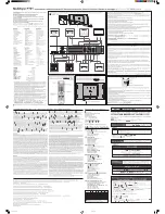
DESCRIPTION OF BLOCK DIAGRAM
1. Video Controller Part.
This part amplifies the level of video signal for the digital conversion and converts from the analog video signal to the
digital video signal using a pixel clock.
The pixel clock for each mode is generated by the PLL.
The range of the pixel clock is from 25MHz to 135MHz.
This part consists of the Scaler, ADC and TMDS receiver .
The Scaler gets the video signal converted analog to digital, interpolates input to 1280 X 1024 resolution signal and
outputs 8-bit R, G, B signal to transmitter.
2. Power Part.
This part consists of the 3.3V regulator to convert power which is provided 12V, 5V in Power board and Micom.
5V is provided for LCD panel.
Also, 5V is converted 3.3V by regulator and 3.3V is converted 1.8V by regulator.
Converted power is provided for IC in the main board.
3. MICOM Part.
This part consists of EEPROM IC which stores control data and the Micom.
The Micom distinguishes polarity and frequency of the H/V sync are supplied from signal cable.
The controlled data of each modes is stored in EEPROM.
Содержание L2000C - - 20.1" LCD Monitor
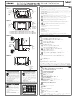
Страница 18: ... 18 WIRING DIAGRAM 6631T12006F 6631T12006L 6631900080A 30P 7P 6P ...
Страница 19: ... 19 EXPLODED VIEW 010 020 060 070 080 090 100 030 110 050 040 ...
Страница 20: ...SCHEMATIC DIAGRAM 23 1 SCALER ...
Страница 21: ... 24 2 POWER WAFER ...
Страница 22: ... 25 3 DC DC BLOCK ...
Страница 23: ...Jun 2006 P NO 38289S0041 Printed in Korea ...