


- 13 -
ADJUSTMENT
All adjustment are thoroughly checked and corrected
when the monitor leaves the factory, but sometimes
several minor adjustment may be required.
Adjustment should be following procedure and after
warming up for a minimum of 10 minutes.
• Alignment appliances and tools.
- IBM compatible PC
- Programmable Signal Generator.
(eg. VG-819 made by Astrodesign Co.)
- E(E)PROM with each mode data saved.
1. Adjustment Start
1) Display any pattern at any Mode.
2) Run alignment program for LB700K on the IBM
compatible PC.
3) Select EEPROM
→
Init
→
Initialize command and
Enter.
4) This will make all data to default state.
5) Select COLOR
→
PRESET START command
and Enter.
2. Adjustment for White Balance
1) Display Black pattern at SXGA/60Hz.
2) Select COLOR
→
BIAS CALIBRATION command
and Enter.
3) No attempt to manually adjust, BIAS data is auto-
matically adjusted and saved to the EEPROM.
4) Display Full White pattern at SXGA/60Hz.
5) Select GAIN CALIBRATION command and Enter.
6) 6500K and 9300K are automatically adjusted and
saved to the EEPROM.
7) Select COLOR
→
PRESET END command and
Enter.
3. Adjustment for EDID
1) Use this procedure only when there is some
probelm on EDID data.
2) Connect the D-sub cable.
3) Select EDID
→
Write EDID[A0] command and
Enter.
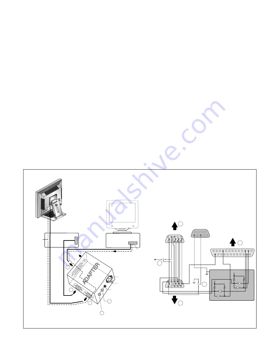
220
IBM
Compatible PC
Video Signal
Generator
PARALLEL PORT
Power inlet (required)
Power LED
ST Switch
Power Select Switch
(110V/220V)
Control Line
Not used
RS232C
PARALLEL
V-SYNC
POWER
ST
VGS
MONITOR
E
E
V-Sync On/Off Switch
(Switch must be ON.)
F
F
A
A
B
B
C
C
15
10
5
5
6
9
1
1
1
14
13
25
6
5V
5V
5V
4.7K
4.7K
4.7K
74LS06
74LS06
OFF
ON
OFF
ON
11
Figure 1. Cable Connection
Содержание Flatron LB700K
Страница 10: ... 10 BLOCK DIAGRAM ...
Страница 21: ... 21 3 ADAPTER BOARD Component Side 4 ADAPTER BOARD Solder Side To apply the AU Module ...
Страница 22: ... 22 5 ADAPTER BOARD Component Side 6 ADAPTER BOARD Solder Side To apply the HYDIS Module ...
Страница 24: ... 24 EXPLODED VIEW 1 2 4 7 3 10 12 11 5 6 9 8 13 14 17 18 15 16 f e d c b a ...
Страница 30: ...SCHEMATIC DIAGRAM 30 1 GM5120 ...
Страница 31: ... 31 2 LVDS ...
Страница 32: ... 32 3 DC DC ...
Страница 33: ... 33 4 CONNECTOR ...
Страница 34: ... 34 5 INPUT SWITCHING ...
Страница 35: ... 35 6 CONTROL KEY ...
Страница 36: ... 36 7 USB ...
Страница 37: ... 37 8 ADAPTER AU Module ...
Страница 38: ... 38 9 INVERTER AU Module ...
Страница 39: ... 39 10 ADAPTER HYDIS Module ...
Страница 40: ... 40 11 INVERTER HYDIS Module ...


