background image

Making 

Repair Process

Revision 

PDP TV

Symptom

A. Picture Problem

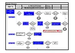
No Picture/Sound OK

1

Check Module pattern 
by using “TILT” key
on SVC R/C

Normal

N

Check

Vs, Va

Y

Normal

N

Check voltage

. -V

Y

. V

SC

. V

ZB

Refer to the Module label for each voltage

Y

N

1. Check Y-Sus/ Z-Sus Board
2. Replace defective B/D

Check B+ Voltage
on Power Board

/ Control Board

.Check B+(5V)

Y

1.Check Control Board

. LED on
. Crystal(X400)
. 1.8V, 3.3V,1.2V 5V FET
. Rom update

2.Replace Control B/D

<SVC R/C & Pattern>

Check
Sound

Sound

OK

Y

Close

Y

Move 

No Picture/No sound

Section

Check 

LVDS Cable 

Replace

Main B/D

Normal

N

Y

N

Move 

Power problem

Section

Normal

Normal

Move 

Power problem

Section

N

-V

Y

V

SC

V

ZB

First of all, Check whether all of cable between board was inserted properly or not.

(Main B/D

Power B/D, Power B/D

Y-sus B/D,Y-Sus B/D 

Z-Sus B/D,LVDS Cable,Speaker Cable,IR B/D Cable,,,)

Содержание 42PT350R

Страница 1: ...AFETY PRECAUTIONS IN THIS MANUAL CHASSIS PP11K MODEL 42PT350R 42PT350R TD 42PT351R 42PT351R TC North Latin America http aic lgservice com Europe Africa http eic lgservice com Asia Oceania http biz lgservice com Internal Use Only Printed in Korea P NO MFL67002503 1102 REV00 ...

Страница 2: ... Copyright 2011 LG Electronics Inc All rights reserved Only for training and service purposes CONTENTS CONTENTS 2 SAFETY PRECAUTIONS 3 SPECIFICATION 4 ADJUSTMENT INSTRUCTION 6 BLOCK DIAGRAM 12 EXPLODED VIEW 13 CIRCUIT DIAGRAM ...

Страница 3: ...t s Neck Leakage Current Cold Check Antenna Cold Check With the instrument AC plug removed from AC source connect an electrical jumper across the two AC plug prongs Place the AC switch in the on position connect one lead of ohm meter to the AC plug prongs tied together and touch other ohm meter lead in turn to each exposed metallic parts such as antenna terminals phone jacks etc If the exposed met...

Страница 4: ...by part number in accordance with SBOM 5 The receiver must be operated for about 20 minutes prior to the adjustment V Test Method 1 Performance LGE TV test method followed 2 Demanded other specification Safety CE IEC specification EMC CE IEC V Module Specification 1 42 2D HD 42PT350R TA 42PT351R TC NON EU LG Model Name Market Place Brand Model Name 42PT350R TA 42PT351R TC Remark Safety IEC EN60065...

Страница 5: ... China DK Australia BG VHF UHF E2 C69 2 78 VHF UHF C1 C62 C1 C75 CATV S21 S41 1 71 CATV S1 S41 S2 S44 4 Receiving system Upper Heterodyne 5 Video Input 2EA PAL SECAM NTSC Rear 1EA Side 1EA 6 Component Input 2EA Y Cb Cr Y Pb Pr 7 RGB Input 1EA RGB PC 8 HDMI Input 2ea HDMI DTV Only PCM MODE Side HDMI 1 Rear HDMI 1 42 50PT250R TA only 3ea Side HDMI 1 Rear HDMI 2 9 Audio Input 5EA L R Input PC 1EA Com...

Страница 6: ...module is in the circumstance of over 15 C In case of keeping module is in the circumstance of 0 C it should be placed in the circumstance of above 15 C for 2 hours In case of keeping module is in the circumstance of below 20 C it should be placed in the circumstance of above 15 C for 3 hours 3 S W Program Download 3 1 Profile This is for downloading the s w to the flash memory of the IC402 3 2 Eq...

Страница 7: ...on button of the control R C power on TV USB file EPK version must be bigger than downloaded version of main B D It should be only one SW binary file in USB Stick 1 Using Power ON button of the control R C Power on TV 2 Insert the USB memory stick to the SET 3 Display USB loding message then push the Exit Key of control R C 4 Push the MENU Key and move the cusor OPTION of OSD Fig 1 Caution Don t p...

Страница 8: ... After software D L or PCBA manufacturing you can download EDID Data When you adjust Tool Option H6 Model EDID download process is executed automatically If the model don t have HDMI 3 HDMI 3 will be disappeared at OSD Window Caution When you adjust tool option don t connect HDMI or D sub cable If you connect some cable EDID D L process will be failed 7 Adjustment method Before PCBA check have to ...

Страница 9: ...n PP01A B C Chassis it is usi g the EEPROM masking HDCP Key 7 Manual ADC Adjustment Component 1 RGB Caution Do not connect external input cable Adjustment result is applied to SET On Off later Adjustment is done using internal ADC so input signal is not necessary NO Item Condition Hex Data 1 Manufacturer ID GSM 1E6D 2 Version Digital 1 01 3 Revision Digital 3 03 Inch 42PT350R TA Tool option 15 INC...

Страница 10: ...Va Adjustment 1 Connect terminal of D M M to Va pin of P811 connect terminal to GND pin of P811 2 After turning VR502 voltage of D M M adjustment as same as Va voltage which on label of panel right top deviation 0 5 V 8 4 Adjustment of Area option 1 Area Option Adjustment following BOM Including SKD models Tool Option Area Option Option 1 Option 2 Option 3 Available for EU Non EU model Profile Mus...

Страница 11: ...on 192 between R G and B Auto control interface and directions 1 Adjust in the place where the influx of light like floodlight around is blocked Illumination is less than 10ux 2 Measure and adjust after sticking the Color Analyzer CA 100 CA210 to the side of the module 3 Aging time After aging start keep the Power on no suspension of power supply and heat run over 5 minutes Above optical character...

Страница 12: ... 12 LGE Internal Use Only Copyright 2011 LG Electronics Inc All rights reserved Only for training and service purposes BLOCK DIAGRAM ...

Страница 13: ... special safety related characteristics These parts are identified by in the Schematic Diagram and EXPLODED VIEW It is essential that these special safety parts should be replaced with the same components as recommended in this manual to prevent X RADIATION Shock Fire or other Hazards Do not modify the original design without permission of manufacturer IMPORTANT SAFETY NOTICE A10 A9 LV1 A12 A21 A2...

Страница 14: ...32 SIDE_HDMI 14 NC 13 CEC 5 DATA1_SHIELD 20 JACK_GND 12 CLK 11 CLK_SHIELD 2 DATA2_SHIELD 19 HPD 18 5V_POWER 10 CLK 4 DATA1 1 DATA2 17 DDC CEC_GND 9 DATA0 8 DATA0_SHIELD 3 DATA2 16 SDA 7 DATA0 6 DATA1 15 SCL R105 10K SIDE_HDMI 5V_HDMI_3 JK103 PEJ027 01 6B 7B 5 4 7A 6A 3 R142 100 NONE_RGB R143 100 NONE_RGB R144 100 NONE_RGB R150 100 NONE_RGB R180 5 1 R181 5 1 R148 10K R174 10K R179 12K R178 12K R154...

Страница 15: ...6V R225 330 1 10W 1 3 3V_MPLL C205 0 01uF 25V R219 10K KEY1 L203 0 1 4W 5 M5V_ON R226 4 7K R221 4 7K L201 MLB 201209 0120P N2 120 ohm ERROR_DET P200 SMAW200 H18S1 14 9 4 18 13 8 3 17 12 7 2 16 11 6 1 15 10 5 19 5V_MULTI 5V_MULTI 5V_ST IC201 MP2305DS 3 SW 2 IN 4 GND 1 BS 5 FB 6 COMP 7 EN 8 SS R236 100 17V_TI R222 4 7K R247 READY 1 8V_DDR 3 3V_MPLL C208 100uF 16V IC200 AP2121N 3 3TRE1 1 GND 2 VOUT 3...

Страница 16: ...PGND_CD_2 39 OUT_C 40 PVDD_C_1 41 PVDD_C_2 42 BST_C 43 BST_B 44 PVDD_B_1 45 PVDD_B_2 46 OUT_B 47 PGND_AB_1 48 PGND_AB_2 C301 1000pF 50V C302 0 1uF C304 0 1uF C313 0 047uF C316 4700pF C317 0 1uF C318 1000pF C319 4700pF C320 0 047uF C321 2200pF C322 0 1uF C380 0 1uF C381 0 1uF C382 0 1uF C383 0 1uF C384 0 1uF C385 0 1uF C386 0 1uF C387 0 1uF C388 0 1uF C389 0 1uF C395 0 1uF 16V R304 22 R306 22 R305 ...

Страница 17: ...4 XIN 245 GPIO134 246 GPIO135 247 GPIO138 248 GPIO139 249 GPIO140 250 IRIN 251 HSYNC0 252 VSYNC0 253 HSYNC1 254 VSYNC1 255 CEC 256 HWRESET DDR2_WEZ MNT_R_AMP R429 47 1 16W 5 C400 0 01uF 25V TMDS2_RX1 HPD_MST_2 R450 4 7K V_REF C418 2 2uF IR COMP2_Y R469 100 C430 0 047uF R455 1K SPI_DO R421 47 R414 22K 3 3V_MST R400 4 7K TMDS2_RX0 KEY2 MUTE_LINE C441 1000pF IC403 3 LGE4768A Matrix Only SD Divx_RM_NO...

Страница 18: ......

Страница 19: ...Board Control Board Check B 5V Y 1 Check Control Board LED on Crystal X400 1 8V 3 3V 1 2V 5V FET Rom update 2 Replace Control B D SVC R C Pattern Check Sound Sound OK Y Close Y Move No Picture No sound Section Check LVDS Cable Replace Main B D Normal N Y N Move Power problem Section Normal Normal Move Power problem Section N VY VSC VZB First of all Check whether all of cable between board was inse...

Страница 20: ... Picture No Sound Repair Process Check Module pattern by using TILT key on SVC R C Normal N Check Sound Sound OK Y N Move No Picture Sound Ok Section Close Y Check LVDS Cable Replace Main B D Normal Y N Replace Main B D Normal Check Input signal RF Cable connection SCART Cable connection HDMI Cable connection Component Cable 2 Normal Y N Repair Replace IR B D ...
Страница 21: ...Check voltage VY VSC Y Sus B D Normal Picture Replace Y Sus B D Normal Picture Y N 1 Check Control B D 2 Replace Board Normal Picture Check Y Drive B D Replace B D Y Close N Dark Picture Normal Picture Y Replace Module N Close 1 Check Z Sus Board 2 Replace Board Check Picture mode setting Picture Noise Normal Picture Y N Close Y N Check RF Cable Connection Check Tuner Replace Normal Picture Check ...

Страница 22: ...her equipments have problem or not By connecting RF Cable at other equipment DVD Player Set Top Box Different maker TV etc SVC Bulletin Replace Main B D Check Tuner soldering Normal Picture Y N Y Close Normal Picture Y Close By using signal level meter Signal strength Normal over 50 Signal Quality Normal over 50 Normal Picture Y Contact with signal distributor or broadcaster Cable or Air N N Norma...

Страница 23: ...f Main B D doesn t cause N Y Close 1 Connector re connection 2 Eliminate foreign material on Connector N CTRL B D Control board Check connection of Connector COF TCP on CTRL B D X B D Check connection of Connector FPC on Y Drive B D 1 Connector re connection 2 Eliminate foreign material on FFC 1 Check Y Drive B D 2 Replace Board Normal Picture N Y Close Replace Module 1 Check CTRL B D 2 Replace Bo...

Страница 24: ... Key On Remote control Normal Close Y N Y Repair Replace IR B D N Check Power cord was inserted properly N Normal Close Y Check ST BY 3 5V on Power Board Normal Voltage N Normal Signal Y Check Power B D Replace Power B D Check AC DET Signal on Power B D Check RL_ON Signal on Power B D N Normal Signal Y Check Main B D Replace Main B D Check the other pin s Output voltage on Power B D Normal Close Y...

Страница 25: ...ED Green Y Check Power B D Replace Power B D 1 Check Y Sus Z Sus Board especially Short or Open 2 Replace defective B D To check Power B D Protection Check Power Off History RCU Off 7 Turn off Under watching Off Timer Set Off timer Function off KEY Off 2HOUR Off NO Signal Off Y N Don t appear Power Off History Move No Power problem Section This is not problem Normal operation ...

Страница 26: ...ose Y 2 Sound distortion sound drop Check Input signal Cable connection Cable open RF external HDMI SCART Normal Sound Y Close Check AVL off on Clear voiceⅡ off on Y Normal Sound N Close N Problem in all input Problem in external input Case 2 SCART HDMI Check whether Problem happen in same output of other equipments or not By connecting same output cable of other equipment DVD Player Set Top Box d...

Страница 27: ...e Explain the customer cause is interference from light in room Check R C Operating When turn off light in room Check Replace Baterry of R C Check Repair Cable connection Connector solder Normal operating Check B 5V On Main B D Normal Voltage Close N N Check 5v on Power B D Replace Power B D or Replace Main B D Power B D don t have problem Check IR Output signal Normal Signal N Y Repair Replace IR...

Страница 28: ... 2 Image sticking 3 Mal discharge 4 Module defect V Line Bar H Line Bar 5 In case of no picture you can judge defect cause Module or Main B D If patterns appear defect cause is Main B D Tilt Key Making Revision PDP TV Symptom A Picture Problem Check Module pattern by Tilt key Repair Process Reference data Item A1 ...

Страница 29: ...101 on Control B D Check LED On If LED light doesn t appear check Crystal X101 output Check 3 3V 5V 1 8V FET Check MCM at VS_DA by using Multi meter Checking Method Check Crystal X101 3 3 V 5 V 1 8 V Check LED On Check Input voltage GND Check Crystal X101 Check oscillation of Crystal Normal 100 MHZ 1 6v MCM Check point VS_DA GND Normal 3 3V Check MCM ...

Страница 30: ... Checking method Repair Process Reference data A15 Check by using Rom Label on control board Rom ver Label Check by using SVC Remocon Press In start Press 0000 Select Panel option Pop up Module Rom ver Refer to the Module Rom upgrade manual for Rom upgrade USB Type Jig ...

Страница 31: ...B D Panel 2 Check Y Sus B D 3 Replace Y Sus B D Horizontal Line or Bar 1 Check connection CTRL B D X B D 2 Check CTRL B D 3 Replace CTRL B D Vertical lines or Bar 1 Check connection CTRL B D X B D 2 Check CTRL B D 3 Replace CTRL B D Regular vertical lines To action defects description Symptom picture First of all Check whether all of cable between board was inserted properly or not Next Check whet...

Страница 32: ... 96 Out Put COF Type 1 Check foreign Connection status 2 Check bad soldering on Chip resistance Defect symptom 192 Out Put TCP Type TCP Tape Carrier Package is film for IC connect with Electrode pattern Direct Bonding on X B D FPC Type Connector to connect between Electrode PAD Of PANEL and Y Drive B D Z Sus B D ...

Страница 33: ...D Main B D P813 P1100 5V Error_DET 8 7 6 17 15 16 14 No High 3 3V 5V RL_ON High 3 3V 5V AC DET 5V STBY 5V Check the other pin s output High 3 3V 5V Vs ON High 3 3V 5V M5_ON Remark Spec Checking Point P814 1 17V 2 17V 3 GND 4 GND 5 5V 6 5V 7 5V 8 Error_DET 9 GND 10 GND 11 GND 12 GND 13 STBY 14 STBY 15 RL_ON 16 AC_DET 17 M_ON 18 AUTO_GND Wafer SMAW200 H18S2 ...

Отзывы: