background image

- 29 -

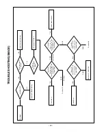
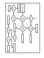
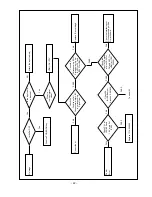
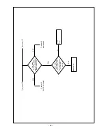
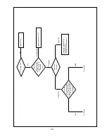
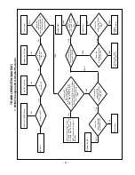
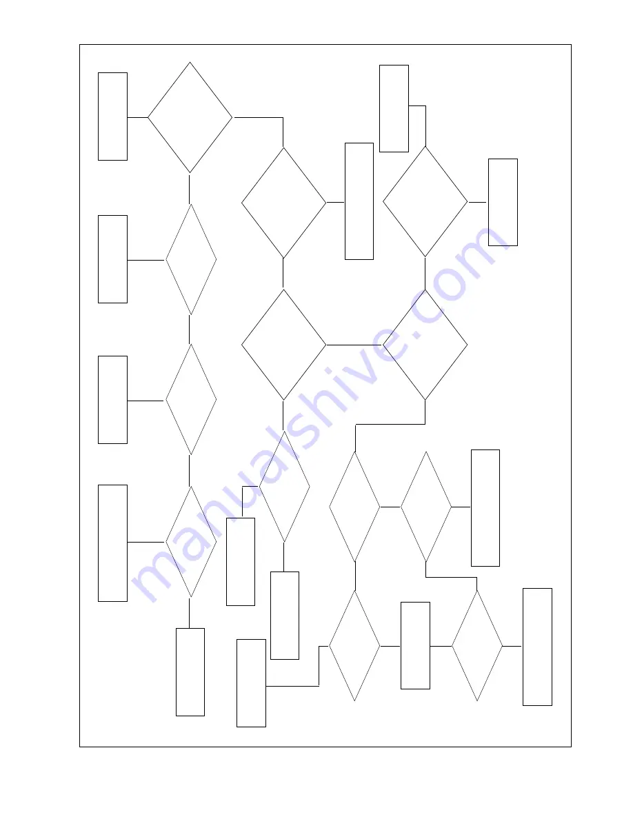
Check the

Condition of all 

Connectors, wafers, I2C

In corresponding

Signal flow?

Check the 

input LR signal 

at pin no 5,12 or 7,10 of 

IC907 for AV1,2 

respectively

Check the 

input Analog LR 

across R616,615

Check audio

output at MSP

across R655,656,657

And 605.

Check the 

supply voltage 8V 

across L601-602

Is Volume level 

Of the set  0?

Is Mute ON?

Check 

12V at pin 9 of 

IC907

Check the 

PWM output of NSP 

across R325-328

Check the 

Amplifier output level 

At L300-303

Check 

3.3V supply across 

L305 and 2.5V at

L304

Check 18V 

supply at pin 55and 

pin 30 of 

AMP

Is the Set ON?

Correct them

Replace the MSP

Power Error

Increase the Volume

Turn OFF the Mute

Replace IC907

Power Error 

Power Error 

Replace NSP

Push the POWER ON key

There may be some 

error in PC input.

Replace TAS5122(amp)

Check the interfacing

Ciruit of SCART1/2.

No Audio

FAIL

PASS

PASS

FAIL

FAIL

PASS

PASS

FAIL

FAIL

PASS

PASS

PASS

FAIL

PASS

Yes

FAIL

PASS

FAIL

PASS

PASS

PASS

FAIL

FAIL

FAIL

PASS

FAIL

3. SCART(A

V1/2) Audio

Содержание 42LP1D-EA

Страница 1: ... TV SERVICE MANUAL CAUTION BEFORE SERVICING THE CHASSIS READ THE SAFETY PRECAUTIONS IN THIS MANUAL CHASSIS ML 03JB MODEL 42LP1D EA website http biz LGservice com e mail http www LGEservice com techsup html ...

Страница 2: ...PRODUCT SAFETY 3 SPECIFICATION 6 TIMING CHART 11 ADJUSTMENT INSTRUCTION 12 SVC REMOCON 19 TROUBLE SHOOTING 20 BLOCK DIAGRAM 30 WIRING DIAGRAM 37 EXPLODED VIEW 38 EXPLODED VIEW PARTS LIST 39 REPLACEMENT PARTS LIST 40 SVC SHEET ...

Страница 3: ...Current Cold Check Antenna Cold Check With the instrument AC plug removed from AC source connect an electrical jumper across the two AC plug prongs Place the AC switch in the on position connect one lead of ohm meter to the AC plug prongs tied together and touch other ohm meter lead in turn to each exposed metallic parts such as antenna terminals phone jacks etc If the exposed metallic part has a ...

Страница 4: ...vely obtain and wear a commercially available discharging wrist strap device which should be removed to prevent potential shock reasons prior to applying power to the unit under test 2 After removing an electrical assembly equipped with ES devices place the assembly on a conductive surface such as aluminum foil to prevent electrostatic charge buildup or exposure of the assembly 3 Use only a ground...

Страница 5: ...not shiny reheat them and if necessary apply additional solder Fuse and Conventional Resistor Removal Replacement 1 Clip each fuse or resistor lead at top of the circuit board hollow stake 2 Securely crimp the leads of replacement component around notch at stake top 3 Solder the connections CAUTION Maintain original spacing between the replaced component and adjacent components and the circuit boa...

Страница 6: ...SPECIFICATION NOTE Specifications and others are subject to change without notice for improvement 3 General Specification No Item Specification Remark Min Typ Max Unit 1 Video Input applicable system 1 PAL SECAM BG EU Non EU PAL Market 2 PAL SECAM DK 3 PAL I 4 SECAM L L 5 NTSC M 6 PAL N M 6 7 South America Market 7 NTSC M 7 South America except other NTSC Market 2 AV input System 1 PAL 2 SECAM 3 N...

Страница 7: ...tage Vrms Operating Current mA 14 Weight 21 5 22 5 23 5 kg TV Speaker 15 Size of Outline H 501 6mmX W 1051mmX D 109mm mm TV Speaker 16 SPEAKER Impedance 8 Tweeter 8 Regularity Output Power 15 15 W 17 Power On Time 9 Sec Stand by power on time 18 RS 232C 1 EA S W Download Half Scart 1 EA EU Full Scart 1 EA EU RF Input Analogue 1 EA UK 2 EA Non UK 2 TUNER DTV ID TV Only UK AV Input 1 EU Side 2 Non E...

Страница 8: ... 2D 78 0A 36 E9 A3 56 49 9B 25 20 48 4B 20 00 00 01 01 01 01 01 01 01 01 01 01 01 30 01 01 01 01 01 01 01 1D 80 18 71 1C 16 20 58 2C 40 25 00 C4 8E 21 00 00 9E 8C 0A D0 8A 20 E0 2D 10 50 10 3E 96 00 C4 8E 21 00 00 18 00 00 00 FC 00 33 60 32 4C 50 31 44 2D 19 0A 20 20 20 20 00 00 00 FD 70 00 38 4B 1F 46 08 00 0A 20 20 20 20 20 20 01 FC 80 02 03 21 71 46 85 04 02 01 03 00 23 09 07 07 23 90 09 07 07 ...

Страница 9: ...Scart Pin Signal Signal Level Impedance 1 Audio Output B right 0 5 Vrms 1 2 Audio Input B right 0 5 Vrms 10 3 Audio Output A left 0 5 Vrms 1 4 Ground audio 5 Ground blue 6 Audio input A left 0 5 Vrms 10 7 Blue input 0 7 V 75 8 Function Select AV control High 9 5 12V AV Mode Mid 5 8V Wide Screen 10 Low 0 2V TV Mode 9 Ground Green 10 Comms Data 2 11 Green input 0 7 V 75 12 Comms Data 1 13 Ground Red...

Страница 10: ... Ground blue 6 Audio input A left 0 5 Vrms 10 7 8 Function Select AV control High 9 5 12V AV Mode Mid 5 8V Wide Screen 10 Low 0 2V TV Mode 9 Ground Green 10 Comms Data 2 11 12 Comms Data 1 13 Ground Red 14 Ground Blanking 15 Red input 0 7 V 75 16 17 Ground Video input Output 18 19 Video output Composite 1V including sync 75 20 Video input Composite 1V including sync 75 21 Common ground Shield ...

Страница 11: ...640 x 480 V Lines 85 008 509 480 1 3 25 6 H Pixels 40 0 37 879 1056 800 40 128 88 800 x 600 V Lines 60 317 628 600 1 4 23 7 H Pixels 49 5 46 875 1056 800 16 80 160 800 x 600 V Lines 75 0 625 600 1 3 21 8 H Pixels 56 25 53 674 1048 800 32 64 152 800 x 600 V Lines 85 061 631 600 1 3 27 9 H Pixels 57 283 49 725 1152 832 32 64 224 832 x 624 V Lines 74 55 667 624 1 3 39 10 H Pixels 65 0 48 363 1344 102...

Страница 12: ... more than 15 minutes with signal maintained Connect input signal to the 24Pin DVI I Jack by using the D sub to DVI I Cable Select INPUT value as DVI PC Default value before adjustment Contrast shipment conditions Brightness shipment conditions Setting to PSM Standard 2 2 3 Operation status check 2 2 3 1 Operation mode Check designated mode accurately operates 2 2 3 2 Check of adjustment status an...

Страница 13: ...K BGIDKM BGIDKM BG I DK M Option1 1 Scart 1 0 SCART OFF 1 SCARTON 2 Sound Curve 0 0 Other area OFF 1 Middle East Vol ON 3 HDEV 0 0 HDEV OFF 1 HDEV ON No Item Condition Remark 4 OSD Lan 0 0 Eng Only 1 1 7 countries 7 countries in West Europe 2 11 countries West Europe Northern Europe 3 Farsi 4 Arab 5 Urdu 6 English Hindi 7 East Asia4 8 English Tha 9 English China Option2 1 Download 0 0 Download dis...

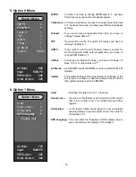
Страница 14: ...GB PC PW Version 3 00 Ucom Version 3 00 Input RGB PC PW Version 3 00 Ucom Version 3 00 If you press the menu button of remote control and the menu key of keypad till more 5 seconds simultaneously The service menu OSD will appear This service menu contain the RGB MSP NSP menus and 3 optional menus that is Option 0 1 2 If you want to correct the difference of colour gain of AD converter or set the P...

Страница 15: ... Volume Nicam Prescale decides input signal level of Nicam audio signal Scart Prescale decides output signal level to speaker volume which is coming from SCART input IIS3 Prescale decides signal level of IIS3 signal line It decides output signal level to speaker volume which is coming from Digital sound input Scart1 Volume decides output level of Scart1 Full Scart2 Volume decides output level of S...

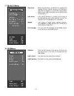
Страница 16: ...etext If you want to see broadcasted text then you have to change Teletext data to 1 TOP If you want to use the Top option in Teletext you have to change Top data to 1 ACMS If you want to use the auto channel memory system for storing channels while auto programming you have to change ACMS data to 1 I IISave In Europe and Eastern Europe you have to change I II Save to 0 For other areas it is 1 A2 ...

Страница 17: ...d for updating the software the main Micom should not communicate with other Ics therefore to cut off the communication between main Micom and other Ics we set the value of Download to 1 SVC Cursdr This setting disables or enables the working of navigation arrow keys while servicing the set The value is set to 0 for disable and 1 for enable RS232C This option is used while updating Scalar uControl...

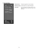
Страница 18: ...sh X STUDIO ISP Press to start ISP Input AV1 PW Version 2 09 Ucom Version 1 07 Input AV1 PW Version 2 09 Ucom Version 1 07 X Studio Version It shows the programme version of X studio X Studio Language This field shows the X studio OSD language X Studio ISP This field shows that X studio memory will be ready for ISP after selecting this option and pressing ok ...

Страница 19: ...put To check the front AV To move channel up down or to select a function displayed on the screen To adjust the volume or accurately control a specific function To set a specific function or complete setting To move the channel down in the PIP screen To use as a red key in the teletext mode To move the channel in the PIP screen To use as a green key in the teletext mode To switch between the main ...

Страница 20: ...ut signal mode Check the Input Y Cb Cr At the pin no 5 7 9 of IC AN15865 on Jack board Check the Condition of all Connectors wafers I2C In component Signal flow Power Error Replace IC1 AN15865 To sheet 24 To sheet 25 Yes NO Yes FAIL PASS component PASS S Video FAIL FAIL PASS PASS PASS FAIL NO Check the output YUV at R 418 415 412 respectively Check 9V Across L401and 5V across L404 and L402 ...

Страница 21: ... is the input signal mode Check main CVBS at R303 Check Secondary CVBS at R434 for PiP Check 9V Across L401and at pin 3 of IC100 5V across L404 L402 Check 9V Across L401and at pin 3 of IC100 5V across L404 L402 Check the input video signal at pin 48 50 52 54 60 of AN15865 For RF AV1 2 3 IDTV Resp Check the Condition of all Connectors wafers I2C In corresponding Signal flow Yes NO Yes FAIL PASS FAI...

Страница 22: ...nd IC203 for HDMI Check the Condition of all Connectors wafers I2C In corresponding Signal flow Power Error Replace IC1 AN15865 To sheet 25 Yes Yes Yes FAIL FAIL FAIL PASS PASS PASS PASS PASS FAIL FAIL Check the interfacing ckt Of corresponding mode On jack board NO Check the input TMDS signal at pins 39 52 for DVI and 58 71 for HDMI of IC601 SiI9021 Check 24 Bit RGB output Across AR 601 606 Check...

Страница 23: ...rect them What is the input signal mode Check the i p RGB HV signal At the pin no 72 76 for X studio and 1 2 78 80 For PC of AN15865 Check the Condition of all Connectors wafers I2C and slots In corres Ponding Signal flow Power Error Replace IC1 AN15865 To sheet 24 Yes NO Yes FAIL PASS FAIL FAIL PASS PASS PASS FAIL NO Check the output YUV at R 418 415 412 respectively Check 9V Across L401and 5V ac...

Страница 24: ...of ADC X98014 across RA500 501 Check the 3 3V supply volt across L503 L504 And clock frequency at pin 39 40 of ADC From sheet 23 From sheet 20 To sheet 25 DVI PC X Studio To sheet 25 component Power Error Replace ADC PASS PASS PASS FAIL FAIL ...

Страница 25: ...put for PiP at pin 37 41 45 47 for main image at pin 48 46 42 38 of IC902 LVDS IC check 3 3Vdd and 2 5Vdd across respectively LIP2 and LIP1 check the 3 3Vdd across CF12 and 1 8Vdd across CF27 CF33 and 13 5 MHz at pin 191 192 of Froudja Replace Froudja Replace PW181 Power Error Power Error Replace LVDS Replace IEP Crystal or Power Error Replace VSP9437B Crystal or Power Error Crystal or Power Error...

Страница 26: ...cross RA18 20 22 if PiP is digital or CVBS at R434 if PiP is RF AV at AN15865 Is PiP mode ON What is the PIP input Push PiP key Change the input for PiP Follow the corresponding Troubleshooting Procedure for same mode To sheet 25 To sheet 21 NO Not Supported PASS FAIL Any other DTV RF AV Supported Yes ...

Страница 27: ... supply across L305 and 2 5V at L304 Check the PWM output of NSP across R325 328 Is Mute ON Is the Set ON Correct them Replace NSP Power Error Replace TAS5122 amp Power Error Check the Amplifier output level At L300 303 There may be some error in Audio source Increase the Volume Turn OFF the Mute Push the POWER ON key Check the interfacing ciruit of PC audio Analog Tuner Front AV board Side AV boa...

Страница 28: ... NSP across R325 328 Check the Amplifier output level At L300 303 Check 3 3V supply across L305 and 2 5V at L304 Check 18V supply at pin 55and pin 30 of AMP Is the Set ON No power LED indicator off Replace the MSP Power Error Increase the Volume Turn OFF the Mute Replace IC907 Power Error Power Error Replace NSP Push the POWER ON key There may be some error in PC input Replace TAS5122 amp Check th...

Страница 29: ... output of NSP across R325 328 Check the Amplifier output level At L300 303 Check 3 3V supply across L305 and 2 5V at L304 Check 18V supply at pin 55and pin 30 of AMP Is the Set ON Correct them Replace the MSP Power Error Increase the Volume Turn OFF the Mute Replace IC907 Power Error Power Error Replace NSP Push the POWER ON key There may be some error in PC input Replace TAS5122 amp Check the in...

Страница 30: ... COM0 1SCL SDA M COM0 1SCL SDA S RX TX RX TX P RX TX M RX TX S 656 8BIT Y C H V SYNC Digital 656 8BIT Y C H V SYNC SW 656 8BIT Y C H V SYNC TEXT R G B FB M2 CVBS R G B FB YUV 4 2 2 16BIT CLK H V SYNC V G RGB 8 8 8 DE CLK H V SYNC RGB 8 8 8 DE CLK H V SYNC RGB 8 8 8 IIC PWR0 1 VFD CS DA CLK PANEL S W INV CTL AV ID IR SND MUTE H V SYNC RX TX TMDS DV I TMDS HDMI IIS LR CLK LR CH SCK MCLK IIS DTV IIS ...

Страница 31: ...B G235P COFDM TUNER RF UHF 21 69 MUX IC7 EEPROM 32Kbyte IC306 CIMAX IC102 103 TS BUFFER 74LCV244 TS_DATA 0 7 SYNC CK VALID IC303 DATA S W 74LVC245 IC304 305 ADDR S W 74HCT373 EMI_DATA 0 8 EMI_ADDR 0 14 CN301 CI SLOT TS_DATA 0 7 SYNC CK VALID TS_DATA 0 7 SYNC CK VALID CD CE IRQ WE IORD IOWR WAIT TS_DATA 0 7 SYNC CK VALID I2C I2C I2C To Jack board CVBS YUV PCMDATA PCMCK LRCK UCOM_SIGNAL CPU_SIGNAL P...

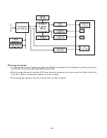
Страница 32: ...CART AV 2 from half SCART and AV 3 from front A V The SCART Audio AV1 AV2 are fed to MSP4410K through the LA7222 switch for selecting appropriate mode while Front LR AV3 is directly fed to the MSP4410K sound processor IC After these operations the audio and video signals follow the same signal flow and processing as in case of RF Analog input 4 Component mode Initially the video signal is fed to t...

Страница 33: ...3 MS_D 0 3 SM_D 0 6 SM_ A 3 7 CF_D 0 6 CF_A 3 7 IIC SCL SDA LRCLK SCLK MCLK AD0 MUTE DISP 0 15 YC SPCK MISO MOSI nSS ACK PCLKO HBLK VBLK SPI_READ SPI_WRITE A 0 10 DQ 0 31 DQM 0 3 CKF SD_CLK B A0 BA1 CS RAS CAS WF AT76C120 Processor 82B 715 AT49BV162A Flash memory CF_50PIN 5IN1_TOP EP1C4F324CB_1 FPGA HY57V643220 PROM 64MB ICS 570B PLL FMS3818 Video DAC UDA 1334BTA Audio DAC 256M SDRAM IIC bus exten...

Страница 34: ...ecture consists of five funda mental programmagble functional elements Configurable Logic Block CLBs Input Output Block IOBs Block RAM Multiplier Blocks Digital Clock Manager DCM The Spartan 3 family features a rich network of traces and switches that interconnect all five functional elements transmitting signals among them Each functional element has an associated switch matrix that permits multi...

Страница 35: ...hen a particular image is selected then the processed 24bit RGB data of corresponding image is retrieved from the SDRAM of FPGA and sent to the video DAC where it is converted into analog RGB signal and sent to the jack board for further processing 5 The horizontal and vertical sync are also provided by the FPGA along with image signal for the synchronization 35 Processor AT76C120 Flash Memory AT4...

Страница 36: ...hen the data is processed by the processor and the I2S data is sent to the audio DAC IC where it is converted into analog AV_L and AV_R signals 3 These analog audio signals are then sent into the jack board for further processing 36 Processor AT76C120 Flash Memory AT49BV162A SDRAM K4S561632E Display Capture FPGA XC2S200E DAC FMS3818 SDRAM HY57V653220C Card connector PROM XCF02S Audio DAC UDA1334BT...

Страница 37: ...g Part List NO PART NO 1 6631T11020A 2 6631T11020Z 3 6631T25023N 4 6631T20034W 5 6631T25024Q 6 6631T25019N 7 6631T25024P 8 6631T20037D 9 6631T20037E 10 6631T11022B 11 6631T11023A 12 6631T20039B 13 6631T12007D 14 6631T20028W 15 6631T20034U 16 6631T20033D 17 6631T20028V 18 6631T20036D 19 6631T25024S 20 6631T25024T 21 6852TAZ012J 22 6852TAZ012N ...

Страница 38: ... 38 EXPLODED VIEW 010 020 080 090 150 110 160 060 030 050 040 180 170 130 120 210 220 100 140 200 190 070 ...

Страница 39: ...71TSTB76A PWB PCB ASSEMBLY SUB 42LP1D EA SUB TOTAL BRAND JACK BOARD ASSY 6871TSTB44A PWB PCB ASSEMBLY SUB 42LP1D EA SUB TOTAL BRAND JACK BOARD ASSY 6871TSTB77A PWB PCB ASSEMBLY SUB 42LP1D EA SUB TOTAL BRAND X STUDIO BOARD ASSY 6871TSTB45A PWB PCB ASSEMBLY SUB 42LP1D EA SUB TOTAL BRAND X STUDIO BOARD ASSY 6871TSTB81A PWB PCB ASSEMBLY SUB 42LP1D EA SUB TOTAL BRAND LOGO BOARD ASSY 6871TSTB48A PWB PCB...

Страница 40: ...NO DESCRIPTION SPECIFICATION C37 0CH6330K416 33PF 50V J NP0 2012 R TP C38 0CH6330K416 33PF 50V J NP0 2012 R TP C518 0CH6220K416 22PF 50V J NP0 2012 R TP C519 0CH6220K416 22PF 50V J NP0 2012 R TP C702 0CH6100K116 10PF 50V D NP0 2012 R TP C92 0CH6220K416 22PF 50V J NP0 2012 R TP C93 0CH6220K416 22PF 50V J NP0 2012 R TP CF19 0CH6100K116 10PF 50V D NP0 2012 R TP CS111 0CH6120K416 12PF 50V J NP0 2012 R...

Страница 41: ...10 X7R 2012 R TP C67 0CH3104K566 0 1UF 50V 10 X7R 2012 R TP C671 0CH3103K516 10000PF 50V 10 B Y5P 2012 DATE 2005 04 25 S AL LOC NO PART NO DESCRIPTION SPECIFICATION C68 0CH3104K566 0 1UF 50V 10 X7R 2012 R TP C701 0CH3104K566 0 1UF 50V 10 X7R 2012 R TP C710 0CH3104K566 0 1UF 50V 10 X7R 2012 R TP C73 0CH3104K566 0 1UF 50V 10 X7R 2012 R TP C76 0CH3104K566 0 1UF 50V 10 X7R 2012 R TP C77 0CH3104K566 0 ...

Страница 42: ...K566 0 1UF 50V 10 X7R 2012 R TP CS49 0CH3104K566 0 1UF 50V 10 X7R 2012 R TP CS50 0CH3104K566 0 1UF 50V 10 X7R 2012 R TP DATE 2005 04 25 S AL LOC NO PART NO DESCRIPTION SPECIFICATION CS51 0CH3104K566 0 1UF 50V 10 X7R 2012 R TP CS52 0CH3104K566 0 1UF 50V 10 X7R 2012 R TP CS53 0CH3104K566 0 1UF 50V 10 X7R 2012 R TP CS54 0CH3104K566 0 1UF 50V 10 X7R 2012 R TP CS55 0CH3104K566 0 1UF 50V 10 X7R 2012 R T...

Страница 43: ... TP SMD C930 0CE477WF6DC 470UF MVK 16V 20 SMD R TP C97 0CE477WF6DC 470UF MVK 16V 20 SMD R TP C99 0CE106SH6DC 10UF MVG 25V 20 SMD R TP CF1 0CE107WF6DC 100UF MVK 16V 20 R TP SMD DATE 2005 04 25 S AL LOC NO PART NO DESCRIPTION SPECIFICATION CF14 0CE107WF6DC 100UF MVK 16V 20 R TP SMD CF16 0CE107WF6DC 100UF MVK 16V 20 R TP SMD CF28 0CE107WF6DC 100UF MVK 16V 20 R TP SMD CF34 0CE107WF6DC 100UF MVK 16V 20...

Страница 44: ...21JT CERATECH 20 DATE 2005 04 25 S AL LOC NO PART NO DESCRIPTION SPECIFICATION L908 6210TCE001P HB 1S2012 121JT CERATECH 20 L909 6210TCE001P HB 1S2012 121JT CERATECH 20 L910 6210TCE001P HB 1S2012 121JT CERATECH 20 LF1 6210TCE001G HH 1M3216 501 CERATEC 3216M LF2 6210TCE001G HH 1M3216 501 CERATEC 3216M LF3 6210TCE001G HH 1M3216 501 CERATEC 3216M LF4 6210TCE001G HH 1M3216 501 CERATEC 3216M LF5 6210TC...

Страница 45: ...22 100 1 10W 5 D R TP R176 0RH1000D622 100 1 10W 5 D R TP DATE 2005 04 25 S AL LOC NO PART NO DESCRIPTION SPECIFICATION R179 0RH4700D622 470 1 10W 5 D R TP R205 0RH3901D622 3 9K 1 10W 5 D R TP R212 0RH4701D622 4 7K 1 10W 5 D R TP R218 0RH4701D622 4 7K 1 10W 5 D R TP R25 0RH4701D622 4 7K 1 10W 5 D R TP R251 0RH1000D622 100 1 10W 5 D R TP R263 0RH1000D622 100 1 10W 5 D R TP R300 0RH0101D622 1 0 1 10...

Страница 46: ...5 D R TP RS70 0RH3301D622 3 3K 1 10W 5 D R TP RS71 0RH3301D622 3 3K 1 10W 5 D R TP RS82 0RH3301D622 3 3K 1 10W 5 D R TP DATE 2005 04 25 S AL LOC NO PART NO DESCRIPTION SPECIFICATION RS83 0RH3301D622 3 3K 1 10W 5 D R TP RS92 0RH1003D622 100K 1 10W 5 D R TP RS93 0RH4701D622 4 7K 1 10W 5 D R TP RS97 0RH3301D622 3 3K 1 10W 5 D R TP R100 0RH1000D622 100 1 10W 5 D R TP R101 0RH1000D622 100 1 10W 5 D R T...

Страница 47: ...CIFICATION RF17 0RH4703D622 470K 1 10W 5 D R TP RF21 0RH1000D622 100 1 10W 5 D R TP RF9 0RH1000D622 100 1 10W 5 D R TP RIP10 0RH1000D622 100 1 10W 5 D R TP RIP17 0RH1000D622 100 1 10W 5 D R TP RS11 0RH4701D622 4 7K 1 10W 5 D R TP RS15 0RH1004D622 1 0M 1 10W 5 D R TP RS2 0RH4701D622 4 7K 1 10W 5 D R TP RS45 0RH1000D622 100 1 10W 5 D R TP RS46 0RH1000D622 100 1 10W 5 D R TP RS47 0RH1000D622 100 1 10...

Страница 48: ... 1K OHM 1 10 W 2012 5 00 R169 0RH1001D622 1K OHM 1 10 W 2012 5 00 R170 0RH1001D622 1K OHM 1 10 W 2012 5 00 DATE 2005 04 25 S AL LOC NO PART NO DESCRIPTION SPECIFICATION R195 0RH1001D622 1K OHM 1 10 W 2012 5 00 R196 0RH1001D622 1K OHM 1 10 W 2012 5 00 R197 0RH1001D622 1K OHM 1 10 W 2012 5 00 R207 0RH0000D622 0 OHM 1 10 W 2012 5 00 D R21 0RH0000D622 0 OHM 1 10 W 2012 5 00 D R22 0RH0000D622 0 OHM 1 1...

Страница 49: ...03G HC 49 SM5H KONY 24 576MHZ XF1 6202VDT002J SX 1 SUNNY 13 500000MHZ DATE 2005 04 25 S AL LOC NO PART NO DESCRIPTION SPECIFICATION XS1 6202VDT002B SX 1 SUNNY SC14 3MHZ 30 IC1 6620F00017C WSDIF 42T WOOYOUNG 2 54P 4 SW1 6600VR1004A SKHMPW 5P CHIP TACT J ALPS SW201 6600VR1004A SKHMPW 5P CHIP TACT J ALPS SW202 6600VR1004A SKHMPW 5P CHIP TACT J ALPS SWS1 6600VR1004A SKHMPW 5P CHIP TACT J ALPS C1210 0C...

Страница 50: ...00 D R1286 0RH0000D622 0 OHM 1 10 W 2012 5 00 D DATE 2005 04 25 S AL LOC NO PART NO DESCRIPTION SPECIFICATION R1288 0RH0000D622 0 OHM 1 10 W 2012 5 00 D LED801 0DLNC0058AA NICHIA NSCW215T R TP WHITE LED802 0DLNC0058AA NICHIA NSCW215T R TP WHITE LED803 0DLNC0058AA NICHIA NSCW215T R TP WHITE LED804 0DLNC0058AA NICHIA NSCW215T R TP WHITE LED805 0DLNC0058AA NICHIA NSCW215T R TP WHITE LED806 0DLNC0058A...

Страница 51: ...566 0 1UF 50V 10 X7R 2012 R TP DATE 2005 04 25 S AL LOC NO PART NO DESCRIPTION SPECIFICATION C330 0CH3104K566 0 1UF 50V 10 X7R 2012 R TP C331 0CH3104K566 0 1UF 50V 10 X7R 2012 R TP C332 0CH3104K566 0 1UF 50V 10 X7R 2012 R TP C333 0CH3104K566 0 1UF 50V 10 X7R 2012 R TP C334 0CH3104K566 0 1UF 50V 10 X7R 2012 R TP C335 0CH3104K566 0 1UF 50V 10 X7R 2012 R TP C336 0CH3104K566 0 1UF 50V 10 X7R 2012 R TP...

Страница 52: ...OC NO PART NO DESCRIPTION SPECIFICATION R361 0RH1002D622 10K OHM 1 10 W 2012 5 00 R38 0RH0332D622 33 1 10W 5 D R TP R39 0RH0332D622 33 1 10W 5 D R TP R40 0RH4701D622 4 7K 1 10W 5 D R TP R405 0RH1802D622 18K 1 10W 5 D R TP R406 0RH1002D622 10K OHM 1 10 W 2012 5 00 R407 0RH2702D622 27K 1 10W 5 D R TP R41 0RH4701D622 4 7K 1 10W 5 D R TP R42 0RH4701D622 4 7K 1 10W 5 D R TP R43 0RH4701D622 4 7K 1 10W 5...

Страница 53: ...M C68H S112 403N1 JST 68P D1 0DR340009AA MBRS340 TP FAIRCHILD NON 40 D4 0DR340009AA MBRS340 TP FAIRCHILD NON 40 IC101 0IMCRSG010A ST3232CDR SGS THOMSON SOP16 DATE 2005 04 25 S AL LOC NO PART NO DESCRIPTION SPECIFICATION IC2 0IMCRNS007C LMS1587CS ADJ NATIONAL SEMI IC2 0IMMRMR027A MX29LV320ATTC 70 MACRONIX 4 IC3 0IZZTSA127A ST 48P 42LP1D EA ST FLASH M IC3 0IZZTSA099A STM 48P 42LP1D EA DIGITAL F IC30...

Страница 54: ...0D622 0 OHM 1 10 W 2012 5 00 D R437 0RH0000D622 0 OHM 1 10 W 2012 5 00 D DATE 2005 04 25 S AL LOC NO PART NO DESCRIPTION SPECIFICATION R438 0RH0000D622 0 OHM 1 10 W 2012 5 00 D R439 0RH0000D622 0 OHM 1 10 W 2012 5 00 D R5 0RH4701D622 4 7K 1 10W 5 D R TP R53 0RH1500D622 150 1 10W 5 D R TP R54 0RH0332D622 33 1 10W 5 D R TP R57 0RH0682D622 68 1 10W 5 D R TP R58 0RH0332D622 33 1 10W 5 D R TP R61 0RH10...

Страница 55: ...F 50V 10 B Y5P 2012 DATE 2005 04 25 S AL LOC NO PART NO DESCRIPTION SPECIFICATION C680 0CH3103K516 10000PF 50V 10 B Y5P 2012 C990 0CH3104K566 0 1UF 50V 10 X7R 2012 R TP CED1 0CH3104K566 0 1UF 50V 10 X7R 2012 R TP CED2 0CH3104K566 0 1UF 50V 10 X7R 2012 R TP CT12 0CH3104K566 0 1UF 50V 10 X7R 2012 R TP CT13 0CH6101K416 100PF 50V J NP0 2012 R TP CT2 0CH3472K516 4700PF 50V K B 2012 R TP CT5 0CH3104K566...

Страница 56: ...1 10W 5 D R TP R261 0RH1000D622 100 1 10W 5 D R TP R262 0RH4701D622 4 7K 1 10W 5 D R TP R263 0RH1000D622 100 1 10W 5 D R TP DATE 2005 04 25 S AL LOC NO PART NO DESCRIPTION SPECIFICATION R264 0RH1000D622 100 1 10W 5 D R TP R265 0RH1000D622 100 1 10W 5 D R TP R266 0RH1000D622 100 1 10W 5 D R TP R268 0RH0682D622 68 1 10W 5 D R TP R274 0RH0222D622 22 OHM 1 10 W 2012 5 00 R275 0RH0752D622 75 1 10W 5 D ...

Страница 57: ...M 1 10 W 2012 5 00 R738 0RH1002D622 10K OHM 1 10 W 2012 5 00 DATE 2005 04 25 S AL LOC NO PART NO DESCRIPTION SPECIFICATION R800 0RH0000D622 0 OHM 1 10 W 2012 5 00 D R801 0RH0000D622 0 OHM 1 10 W 2012 5 00 D R802 0RH0000D622 0 OHM 1 10 W 2012 5 00 D R804 0RH0000D622 0 OHM 1 10 W 2012 5 00 D R858 0RH3302D622 33K 1 10W 5 D R TP R859 0RH2702D622 27K 1 10W 5 D R TP R860 0RH9100D622 910 1 10W 5 D R TP R...

Страница 58: ...100UF MVK 16V 20 R TP SMD DATE 2005 04 25 S AL LOC NO PART NO DESCRIPTION SPECIFICATION C659 0CE106VF6DC 10UF MV 16V 20 R TP SMD S C660 0CE106VF6DC 10UF MV 16V 20 R TP SMD S C668 0CE475WK6DC 4 7UF MVK RC 50V 20 SMD TA C669 0CE475WK6DC 4 7UF MVK RC 50V 20 SMD TA C670 0CE475WK6DC 4 7UF MVK RC 50V 20 SMD TA C671 0CE475WK6DC 4 7UF MVK RC 50V 20 SMD TA C673 0CE106VF6DC 10UF MV 16V 20 R TP SMD S C674 0C...

Страница 59: ...D R467 0RH0000D622 0 OHM 1 10 W 2012 5 00 D R468 0RH0000D622 0 OHM 1 10 W 2012 5 00 D R469 0RH0000D622 0 OHM 1 10 W 2012 5 00 D DATE 2005 04 25 S AL LOC NO PART NO DESCRIPTION SPECIFICATION R471 0RH0000D622 0 OHM 1 10 W 2012 5 00 D R473 0RH4701D622 4 7K 1 10W 5 D R TP R474 0RH4701D622 4 7K 1 10W 5 D R TP R475 0RH0000D622 0 OHM 1 10 W 2012 5 00 D R476 0RH0000D622 0 OHM 1 10 W 2012 5 00 D R480 0RH00...

Страница 60: ...1608 50V 10 R TP X7R C187 0CK104CK56A 0 1UF 1608 50V 10 R TP X7R DATE 2005 04 25 S AL LOC NO PART NO DESCRIPTION SPECIFICATION C188 0CK104CK56A 0 1UF 1608 50V 10 R TP X7R C189 0CK104CK56A 0 1UF 1608 50V 10 R TP X7R C190 0CK104CK56A 0 1UF 1608 50V 10 R TP X7R C191 0CK104CK56A 0 1UF 1608 50V 10 R TP X7R C192 0CK104CK56A 0 1UF 1608 50V 10 R TP X7R C193 0CK104CK56A 0 1UF 1608 50V 10 R TP X7R C194 0CK1...

Страница 61: ...ZTCZ001D RCA SMART 22OHM 1 16 W 5 3 C128 0CK104CK56A 0 1UF 1608 50V 10 R TP X7R DATE 2005 04 25 S AL LOC NO PART NO DESCRIPTION SPECIFICATION C129 0CK104CK56A 0 1UF 1608 50V 10 R TP X7R C133 0CK104CK56A 0 1UF 1608 50V 10 R TP X7R C134 0CK104CK56A 0 1UF 1608 50V 10 R TP X7R C136 0CE476WF6DC 47UF MVK 16V 20 R TP SMD C145 0CE226VF6DC 22UF MV 16V 20 R TP SMD S C147 0CE226VF6DC 22UF MV 16V 20 R TP SMD ...

Страница 62: ... 0RJ3300D677 330 OHM 1 10 W 5 1608 R TP R308 0RJ0222D677 22 OHM 1 10 W 5 1608 R TP R316 0RJ0000D677 0 OHM 1 10 W 5 1608 R TP R317 0RJ0000D677 0 OHM 1 10 W 5 1608 R TP R318 0RJ0000D677 0 OHM 1 10 W 5 1608 R TP R320 0RJ1001D677 1K OHM 1 10 W 5 1608 R TP R322 0RJ1001D677 1K OHM 1 10 W 5 1608 R TP R323 0RJ9100D677 910 OHM 1 10 W 5 1608 R TP R324 0RJ2700D677 270 OHM 1 10 W 5 1608 R TP R325 0RJ3300D677 ...

Страница 63: ......

Страница 64: ......

Страница 65: ......

Страница 66: ......

Страница 67: ...Apr 2005 Printed in Korea P NO 38289S0004A ...

Отзывы: