background image

- 9 -

LGE Internal Use Only

Copyright © 

 LG Electronics. Inc. All rights reserved.

Only for training and service purposes

ADJUSTMENT INSTRUCTION

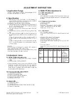
1. Application Range

This spec. sheet applies to LA21B/C Chassis applied LCD TV 

all models manufactured in TV factory.

2. Specification

(1)  Because  this  is  not  a  hot  chassis,  it  is  not  necessary  to 

use an isolation transformer. However, the use of isolation 

transformer will help protect test instrument.

(2) Adjustment must be done in the correct order. 

(3)  The adjustment must be performed in the circumstance of 

25 ±5 °C of temperature and 65±10% of relative humidity if 

there is no specific designation.

(4)  The  input  voltage  of  the  receiver  must  keep  100~240V, 

50/60Hz.

(5)  At first Worker must turn on the SET by using Power Only 

key.

(6)  The receiver must be operated for about 5 minutes prior to 

the adjustment when module is in the circumstance of over 

15 °C

      In case of keeping module is in the circumstance of 0°C, it 

should be placed in the circumstance of above 15°C for 2 

hours

      In case of keeping module is in the circumstance of below 

-20°C,  it  should  be  placed  in  the  circumstance  of  above 

15°C for 3 hours.

[Caution] 

When  still  image  is  displayed  for  a  period  of  20  minutes  or 

longer (especially where W/B scale is strong.

Digital  pattern  13ch  and/or  Cross  hatch  pattern  09ch),  there 

can some afterimage in the black level area

3. Adjustment items

3.1. Main PCBA Adjustments

(1)  ADC  adjustment:  Component  480i,  1080p  /  RGB-PC 

1080p

(2) EDID download: HDMI and RGB-PC

●  Above  adjustment  items  can  be  also  performed  in  Final 

Assembly  if  needed.  Both  Board-level  and  Final  assembly 

adjustment  items  can  be  check  using  In-Start  Menu  (1.

Adjust  Check).  Component  1080p  and  RGB-PC Adjust  will 

be calculated by 480i adjust value.

3.2. Final assembly adjustment

(1) White Balance adjustment

(2) RS-232C functionality check

(3) Factory Option setting per destination

(4) Shipment mode setting (In-Stop)

(5) GND and HI-POT test

3.3. Appendix

(1) Shipment conditions

(2) Tool option menu

(3) USB Download (S/W Update, Option and Service only)

(4) Preset CH Information

4. MAIN PCBA Adjustments

4.1. ADC Adjustment

4.1.1. Overview

▪  ADC  adjustment  is  needed  to  find  the  optimum  black  level 

and gain in Analog-to-Digital device and to compensate RGB 

deviation.

4.1.2. Equipment & Condition

(1) Protocol: RS-232C

(2) Inner Pattern

- Resolution : 1080p(Comp) / 1024*768(RGB)

- Pattern : Horizontal 100% Color Bar Pattern

- Pattern level : 0.7±0.1 Vp-p

4.1.3. Adjustment

4.1.3.1. Adjustment method

-  Connect  to  Jig  by  using  RS-232,  adjust  Component  and 

RGB

● Manual adj (If needed in Final Assembly)

- Required equipment : Adjustment R/C

- Enter Service Mode by pushing “ADJ” key,

-  Enter  Internal ADC  mode  by  pushing  ‘►’  key  at  [6. ADC 

Calibration]

4.1.3.2. Adj. protocol

-  Connect  to  Jig  by  using  RS-232,  adjust  Component  and 

RGB

Protocol CMD 1 CMD 2 Data 1 Data 2

Remark

Enter 

adj 

mode

a

a

00

00

When 

transfer 

the  ‘Mode 

In’,Carry the 

command.

Start 

ADC adj

a

d

00

10

Automatically 

adjustment 

(Use internal 

pattern)

Содержание 42LM3700

Страница 1: ...EL 42LM3700 42LM3700 UC CAUTION BEFORE SERVICING THE CHASSIS READ THE SAFETY PRECAUTIONS IN THIS MANUAL LED LCD TV SERVICE MANUAL North Latin America http aic lgservice com Europe Africa http eic lgservice com Asia Oceania http biz lgservice com Internal Use Only ...

Страница 2: ... LG Electronics Inc All rights reserved Only for training and service purposes CONTENTS CONTENTS 2 PRODUCT SAFETY 3 SPECIFICATION 4 ADJUSTMENT INSTRUCTION 9 TROUBLE SHOOTING 15 BLOCK DIAGRAM 23 EXPLODED VIEW 24 SCHEMATIC CIRCUIT DIAGRAM ...

Страница 3: ...inals etc to be sure the set is safe to operate without damage of electrical shock Leakage Current Cold Check Antenna Cold Check With the instrument AC plug removed from AC source connect an electrical jumper across the two AC plug prongs Place the AC switch in the on position connect one lead of ohm meter to the AC plug prongs tied together and touch other ohm meter lead in turn to each exposed m...

Страница 4: ...nd specification by part number in accordance with BOM 5 The receiver must be operated for about 5 minutes prior to the adjustment 3 Test method 1 Performance LGE TV test method followed 2 Demanded other specification Safety UL CSA IEC specification EMC FCC ICES IEC specification 4 General Specification No Item Specification Remark 1 Receiving System 1 ATSC NTSC M 2 Available Channel 1 VHF 02 13 2...

Страница 5: ...080I 8 1920 1080 33 72 59 94 74 176 HDTV 1080I 9 1920 1080 67 50 60 00 148 50 HDTV 1080P 10 1920 1080 67 432 59 94 148 352 HDTV 1080P 11 1920 1080 27 00 24 00 74 25 HDTV 1080P 12 1920 1080 26 97 23 94 74 176 HDTV 1080P 13 1920 1080 33 75 30 00 74 25 HDTV 1080P 14 1920 1080 33 71 29 97 74 176 HDTV 1080P No Resolution H freq kHz V freq Hz Pixel clock MHz Proposed DDC Remark 1 640 350 31 468 70 09 25...

Страница 6: ...1 60 020 108 0 VESA SXGA O Full HD model Only 8 1360 768 47 712 60 015 85 50 VESA WXGA O 9 1920 1080 67 50 60 00 148 5 HDTV 1080P O Full HD model Only DTV 1 720 480 31 47 60 00 27 027 SDTV 480P 2 720 480 31 47 59 94 27 00 SDTV 480P 3 1280 720 45 00 60 00 74 25 HDTV 720P 4 1280 720 44 96 59 94 74 176 HDTV 720P 5 1920 1080 33 75 60 00 74 25 HDTV 1080I 6 1920 1080 33 72 59 94 74 176 HDTV 1080I 7 1920...

Страница 7: ...920 1080 27 24 74 25 HDTV 1080P Side by Side half Top Bottom 7 1920 1080 33 7 30 74 25 HDTV 1080P Side by Side half Top Bottom No Resolution H freq kHz V freq Hz Pixel clock MHz Proposed 3D input proposed mode 1 1280 720 45 00 60 00 74 25 HDTV 720P Side by Side Top Bottom 2 1920 1080 33 75 60 00 74 25 HDTV 1080I Side by Side Top Bottom 3 1920 1080 27 00 24 00 74 25 HDTV 1080P Side by Side Top Bott...

Страница 8: ...Packing 1 8 4 USB Input 1 Movie No Resolution H freq kHz V freq Hz Pixel clock MHz 3D input proposed mode Proposed 1 1920 1080 33 75 30 74 25 Side by Side HDTV 1080P Top Bottom 2 MPO Picture 3D when selecting the MPO file Automatically 3D on 3 3D Demo in store mode No Resolution H freq kHz V freq Hz Pixel clock MHz Proposed 3D input proposed mode 1 1920 1080 33 75 30 00 74 25 HDTV 1080P Side by Si...

Страница 9: ...ent items 3 1 Main PCBA Adjustments 1 ADC adjustment Component 480i 1080p RGB PC 1080p 2 EDID download HDMI and RGB PC Above adjustment items can be also performed in Final Assembly if needed Both Board level and Final assembly adjustment items can be check using In Start Menu 1 Adjust Check Component 1080p and RGB PC Adjust will be calculated by 480i adjust value 3 2 Final assembly adjustment 1 W...

Страница 10: ...40 45 40 61 40 71 40 81 80 30 01 01 01 01 01 01 02 3A 80 18 71 38 2D 40 58 2C 40 45 00 40 84 63 00 00 1E 66 21 50 B0 51 00 1B 30 50 40 70 36 00 40 84 63 00 00 1E 00 00 00 FD 00 3A 60 3E 1E 53 10 00 0A 20 20 20 20 20 20 00 00 00 FC 70 00 4C 47 20 54 56 0A 20 20 20 20 20 20 20 01 E9 EDID Block 1 Bytes 128 255 80H FFH 0 1 2 3 4 5 6 7 8 9 A B C D E F 0 02 03 19 F1 48 90 22 20 05 04 03 02 01 23 09 57 1...

Страница 11: ...he module surface 80 100 3 Aging time After Aging Start Keep the Power ON status during 5 Minutes In case of LCD Back light on should be checked using no signal or Full white pattern 5 1 2 Equipment 1 Color Analyzer CA 210 NCG CH 9 WCG CH12 LED CH14 2 Adj Computer During auto adj RS 232C protocol is needed 3 Adjust Remocon 4 Video Signal Generator MSPG 925F 720p 204 Gray Model 217 Pattern 49 Only ...

Страница 12: ... coordinate and color temperature Luminance 204 Gray 80IRE Lamp Module Standard color coordinate and temperature using CS 1000 over 26 inch Mode Coordinate Temp uv X Y Cool 0 269 0 273 13 000K 0 0000 Medium 0 285 0 293 9 300K 0 0000 Warm 0 313 0 329 6 500K 0 0000 Standard color coordinate and temperature using CA 210 CH 14 Mode Coordinate Temp uv X Y Cool 0 269 0 002 0 273 0 002 13 000K 0 0000 Med...

Страница 13: ...troller GWS103 4 on 4 GND Test Auto If Test is failed Buzzer operates If Test is passed execute next process Hi pot test Remove A V CORD from A V JACK BOX 5 HI POT test Auto If Test is failed Buzzer operates If Test is passed GOOD Lamp on and move to next process automatically 6 3 Checkpoint 1 Test voltage GND 1 5KV min at 100mA SIGNAL 3KV min at 100mA 2 TEST time 1 second 3 TEST POINT GND Test PO...

Страница 14: ...ow the message Copying files from memory 5 Updating Completed The TV will restart automatically 6 If your TV is turned on check your updated version and Tool option If downloading version is more high than your TV have TV can lost all channel data In this case you have to channel recover If all channel data is cleared you didn t have a DTV ATV test on production line After downloading TOOL OPTION ...

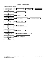
Страница 15: ... or Main board Check Multi Voltage P403 2pin 24V 17pin 12V Replace Power Board Check Inverter Control Error Out P403 18 pin High P403 24 pin low Check Power Board or Module Check IC402 3 7 Output Voltage IC402 2 5V IC403 1 1V IC407 1 5V Q403 3 3V Replace IC402 3 7 Q403 Re download software Check Micom Voltage L404 3 5V Replace L404 Check LVDS Power Voltage Q409 12V Replace Q409 Check Mstar LVDS Ou...

Страница 16: ... 8V Check IF_P N Signal TU3704 10 11 Pin Replace IC3703 Check Mstar LVDS Output Replace Mstar IC101 or Main Board ok ok ok ok No No No No Bad Tuner Replace Tuner 3 Analog TV Video Check RF Cable Signal Check Tuner 3 3V Power L3703 Replace L3703 Check Tuner 1 8V Power IC3703 2 pin 1 8V Check CVBS Signal TU3704 8 Pin Replace IC3703 Check Mstar LVDS Output Replace Mstar IC101 or Main Board ok ok ok o...

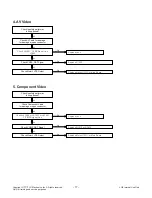
Страница 17: ...eck JK1601 CVBS Signal Line L1603 ok ok ok No Replace Jack ok Check CVBS_DET Signal Replace R1600 No Check Mstar LVDS Output Replace Mstar IC101 or Main Board No Check input signal format Is it supported Check Component Cable for damage or open conductor Check JK1603 or JK1602 or JK1601 Y PB PR signal Line ok ok ok No Replace Jack Check COMP_DET Signal Replace R1612 or R1613 No Check Mstar LVDS Ou...

Страница 18: ...mat Is it supported Check RGB Cable conductors for damage or open conductor Check EDID I2C Signal R1138 R1139 SDA SCL Check JK1104 H V_Sync R G B Signal Line ok ok ok No No re download EDID data Replace Mstar IC101 or Main Board ok Replace Jack Check DSUB_DET Replace R1146 or R1147 No Check Mstar LVDS Output Replace Mstar IC101 or Main Board ok No ...

Страница 19: ...onductor Check EDID R884 R8 I2C Signal Check JK801 JK802 JK803 ok ok ok No No Replace the defective IC or re download EDID data Check HDCP EEPROM IC103 Power I2C Signal Replace the defective IC ok No Replace Jack Check HDMI Signal Check other set If no problem check signal line ok No Check Mstar LVDS Output Replace Mstar IC101 or Main Board ok No Replace Main Board No Check HDMI_DET HPD No ok Repl...

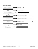
Страница 20: ...1 ok No Check Connector P501 Replace connector if found to be damaged ok No Check speaker resistance and connector damage Replace speaker ok No Off Toggle the Menu Check AMP IC IC501 Power 24V 3 3V No Replace Amp IC IC501 Check Mstar I2S Output IC501 9 10 11 Pin No Check signal line Or replace Mstar IC101 Check Mstar AUDIO_MASTER_CLK R148 No Replace Mstar IC101 or Main Board ok Check AMP I2C Line ...

Страница 21: ...Power L3703 Replace L3703 Check Tuner 1 8V Power IC3703 2 pin 1 8V Check IF_P N Signal TU3700 10 11 Pin Replace IC3703 ok ok ok No No No Bad Tuner Replace Tuner 10 Analog TV Audio Check RF Cable Signal Follow procedure 8 All source audio trouble shooting guide ok Check Tuner 3 3V Power L3703 Replace L3703 Check Tuner 1 8V Power IC3703 2 pin 1 8V Check CVBS Signal TU3700 8 Pin Replace IC3703 ok ok ...

Страница 22: ...gnal Line R1632 R1633 ok ok No Replace Jack Follow procedure 8 All source audio trouble shooting guide Check Component Cable for damage or open conductor Check JK1601 Signal Line R1618 R1617 ok ok No Replace Jack Follow procedure 8 All source audio trouble shooting guide Check Cable conductors for damage or open conductor Check JK1102 Signal Line ok No ok Replace Jack Follow procedure 8 All source...

Страница 23: ...IAL FLASH MXIC 8M bit MX25L8006EM2I LVDS FHD HD 60z A AMP NTP7500 USB2 0 DP DM SPK L R X tal 24MHz FPC 51P FHD I2S SPDIF H P L R L R CVBS Y Pb Pr L R RGB H V Rear TMDS DDR2 Add DDR2 Data SPI AV Side NAND Flash 1Gbit NAND01GW3B2CN6E PCM_A 0 7 TMDS HDMI CVBS L R DDR3 256MB 1Gb Hynic H5TQ1G63DFR DDR3 256MB 1Gb Hynic H5TQ1G63DFR CONTROL IR LED SOFT TOUCH KEY1 KEY2 IR LED_B LG LOGO AT24C1024BN SH T 1Mb...

Страница 24: ...trical and mechanical parts in this chassis have special safety related characteristics These parts are identified by in the Schematic Diagram and EXPLODED VIEW It is essential that these special safety parts should be replaced with the same components as recommended in this manual to prevent X RADIATION Shock Fire or other Hazards Do not modify the original design without permission of manufactur...

Страница 25: ...E_N GPIO113 AB15 PCMWE_N GPIO197 AA22 PCMIORD_N GPIO111 AD22 PCMIOWR_N GPIO109 AD20 PCMCE_N GPIO115 AD21 PCMIRQA_N GPIO105 AC20 PCMCD_N GPIO130 Y18 PCMWAIT_N GPIO100 Y21 PCM_RESET GPIO129 Y22 PCM2_CE_N GPIO131 U21 PCM2_IRQA_N GPIO132 V21 PCM2_CD_N GPIO135 R20 PCM2_WAIT_N GPIO133 T20 PCM2_RESET GPIO134 U22 UART1_TX GPIO43 D4 UART1_RX GPIO44 E4 UART2_TX GPIO65 N25 UART2_RX GPIO64 N24 UART3_TX GPIO47...

Страница 26: ...uF 10V R217 10 C4042 1uF C280 1uF C277 1uF C253 1uF IC101 LGE2111A T8 S7LR2_DIVX_MS10 RXACKP J2 RXACKN J3 RXA0P K3 RXA0N J1 RXA1P K2 RXA1N K1 RXA2P L2 RXA2N L3 DDCDA_DA GPIO24 T5 DDCDA_CK GPIO23 T4 HOTPLUGA GPIO19 V5 HOTPLUGB GPIO20 R5 RXCCKP AE9 RXCCKN AC9 RXC0P AC10 RXC0N AD9 RXC1P AC11 RXC1N AD10 RXC2P AE11 RXC2N AD11 DDCDC_DA GPIO28 AE8 DDCDC_CK GPIO27 AD8 HOTPLUGC GPIO21 AC8 RXDCKP F2 RXDCKN ...

Страница 27: ..._ID PCM_D 1 HP_DET SCART1_MUTE PCM_D 5 PCM_WE SC1_CVBS_IN PCM_IRQA PCM_D 3 CI_CD1 PCM_D 0 PCM_CD CI_TS_DATA 5 PCM_D 2 PCM_A 14 CI_TS_DATA 4 SCART1_Lout PCM_REG HP_ROUT PCM_IOWR CI_TS_DATA 1 PCM_RST CI_CD2 PCM_A 12 CI_TS_VAL CI_TS_DATA 3 PCM_WAIT SCART1_Rout CI_TS_DATA 6 PCM_D 4 PCM_A 8 DTV MNT_VOUT PCM_D 7 CI_DET PCM_OE SIDE_HP_MUTE CI_TS_DATA 7 S2_RESET PCM_IORD PCM_A 11 2011 07 07 TP_NON_EN 3 GP...

Страница 28: ...uF R440 5 6K 12V 15V 3 5V_ST C445 0 1uF 16V OPT 24V C404 0 1uF 16V R412 0 OPT 3 3V_Normal 100 R420 ERROR_OUT INV_CTL R180 10K OPT R489 10K R446 10K OPT R441 56K 1 16W 1 R463 10K OPT 2 5V_Normal C412 0 1uF 16V PD_ 12V R402 100 R415 100 3 3V_Normal R438 22K R443 10K A_DIM R457 4 3K 1 16W 1 C472 22uF 10V L415 3 6uH NR8040T3R6N IC408 1 APX803D29 PWR_DET_ON_DIODES 1 GND 3 VCC 2 RESET IC409 1 APX803D29 ...

Страница 29: ... 50V C2401 0 1uF L2404 BLM18PG121SN1D 11_SUB L2401 BLM18PG121SN1D SENSOR_SDA P2402 12507WR 15L 11_SUB 1 2 3 4 5 6 7 8 9 10 11 12 13 14 16 15 3 5V_ST C2402 0 1uF S T_SDA C2404 1000pF 50V R2405 10K 1 JP2407 P2401 12507WR 10L 12_SUB 1 2 3 4 5 6 7 8 9 10 11 JP2409 LED_B LG_LOGO JP2408 C907 18pF 50V OPT 3 3V_Normal C2403 0 1uF 16V IR_OUT C2405 0 1uF 16V 11_SUB KEY1 JP2410 3 5V_ST R2426 3 3K Q2405 MMBT3...

Страница 30: ...OPT D1451 RCLAMP0502BA OPT C1450 22uF 16V USB_2 USB2_OCD R1453 47 USB_2 JK1451 3AU04S 305 ZC LG USB_2_NORMAL 1 2 3 4 5 IC1451 AP2191DSG EAN61849601 USB_2 3 IN_2 2 IN_1 4 EN 1 GND 5 FLG 6 OUT_1 7 OUT_2 8 NC 5V_USB SIDE_USB1_DM USB1_CTL SIDE_USB1_DP C1455 0 1uF USB_2 L1451 CIS21J121 JK1450 1 3AU04S 345 ZC H LG USB_1_32LS3500 1 2 3 4 5 R1456 10K USB_2 L1451 1 MLB 201209 0120P N2 120 ohm JK1451 1 3AU0...

Страница 31: ...13 5 D1_GND 20 SHIELD 12 11 2 D2_GND 19 18 10 CK 4 D1 1 D2 17 9 D0 8 D0_GND 3 D2 16 7 D0 6 D1 15 HDMI_CEC D0 _HDMI1 5V_DET_HDMI_1 D0 _HDMI1 D0 _HDMI4 CK _HDMI4 R884 2 7K JK803 EAG62611201 HDMI_SIDE 14 13 5 D1_GND 20 BODY_SHIELD 12 11 2 D2_GND 19 18 10 CK 4 D1 1 D2 17 9 D0 8 D0_GND 3 D2 16 7 D0 6 D1 15 DDC_SCL_1 5V_HDMI_4 DDC_SCL_2 R828 10K HDMI_2 R885 2 7K HDMI_2 R835 3 3K HDMI_SIDE D1 _HDMI1 DDC_...

Страница 32: ...SUB_G C1107 100pF 50V NON_CI_CAP_PC_AUDIO C1121 100pF 50V SPDIF_OPTIC RGB_DDC_SDA R1108 15K PC_AUDIO JK1103 2F01TC1 CLM97 4F SPDIF_OPTIC 3 VIN 2 VCC 1 GND 4 SHIELD R1111 10K PC_AUDIO R1104 10K OPT DSUB_HSYNC R1140 2 2K RGB_PC DSUB_VSYNC DSUB_B R1146 10K RGB_PC C1110 10uF 16V OPT 5V_Normal C1109 22uF 16V OPT R1103 470K PC_AUDIO C1131 0 1uF 16V SPDIF_OPTIC SPDIF_OUT PC_R_IN RGB_DDC_SCL R1139 2 2K RG...

Страница 33: ...F COMMERCIAL R1001 0 RS 232C_IC_Bypass R1000 0 RS 232C_IC_Bypass C1001 0 1uF COMMERCIAL P1000 12507WR 04L 1 VCC 2 PM_RXD 3 GND 4 RM_TXD 5 GND C1004 0 1uF COMMERCIAL IC1000 MAX3232CDR EAN41348201 COMMERCIAL 3 C1 2 V 4 C2 1 C1 6 V 5 C2 7 DOUT2 8 RIN2 9 ROUT2 10 DIN2 11 DIN1 12 ROUT1 13 RIN1 14 DOUT1 15 GND 16 VCC JP1000 PM_RXD 3 5V_ST C1000 0 33uF COMMERCIAL R1003 100 R1002 100 JP1002 JP1001 JP1003 ...

Страница 34: ...04 10K OPT L702 70 ohm FHD L701 BLM18SG700TN1D 70 ohm HD AUO_GND LGD_NC LVDS_SEL 30Pin LVDS Connector For HD 60Hz_Normal LVDS for large inch 51Pin LVDS Connector For FHD 60Hz RXB3 RXA4 RXA0 RXB4 RXB1 RXB1 RXA4 RXB3 RXA4 RXA2 RXB3 RXB2 MIRROR FOR FHD REVERSE 8bit RXA0 RXA3 RXB0 RXA2 RXACK RXA1 RXA4 RXB1 RXB3 RXA2 RXB2 RXB4 RXB3 RXB0 MIRROR RXB3 RXB2 RXBCK RXACK RXB3 RXB1 RXA1 RXA0 RXB2 RXB4 RXA2 RX...

Страница 35: ...2 A4 P8 A5 P2 A6 R8 A7 R2 A8 T8 A9 R3 A10 AP L7 A11 R7 A12 BC N7 A13 T3 NC_5 M7 BA0 M2 BA1 N8 BA2 M3 CK J7 CK K7 CKE K9 CS L2 ODT K1 RAS J3 CAS K3 WE L3 RESET T2 DQSL F3 DQSL G3 DQSU C7 DQSU B7 DML E7 DMU D3 DQL0 E3 DQL1 F7 DQL2 F2 DQL3 F8 DQL4 H3 DQL5 H8 DQL6 G2 DQL7 H7 DQU0 D7 DQU1 C3 DQU2 C8 DQU3 C2 DQU4 A7 DQU5 A2 DQU6 B8 DQU7 A3 VREFCA M8 VREFDQ H1 ZQ L8 VDD_1 B2 VDD_2 D9 VDD_3 G7 VDD_4 K2 VD...

Страница 36: ...11 NC_3 12 B3 3 3V 13 B4 1 23V 14 NC_4 15 GND 16 ERROR 17 SYNC 18 VALID 19 MCLK 20 D0 21 D1 22 D2 23 D3 24 D4 25 D5 26 D6 27 D7 28 SHIELD TU3704 TDSH T101F SI2176_TW_2INPUT_H 5 B1 3 3V 11 DIF N 2 RESET 10 DIF P 4 SDA 1 RF_S W_CTL 9 IF_AGC 8 CVBS 3 SCL 7 B2 1 8V 6 SIF 12 SHIELD R3751 220 TU_BUFFER R3752 220 TU_BUFFER R3766 1 R3774 470 TU_BUFFER R3747 20K 1005 FULL_NIM_BCD R3776 10K FULL_NIM_BCD R37...

Страница 37: ...CT 4 L 5 GND 1 R 3 3V_Normal R1504 10K HEAD_PHONE C1503 1000pF 50V OPT HP_LOUT R1503 1K HEAD_PHONE HP_DET 3 5V_ST HP_ROUT SIDE_HP_MUTE R1501 1K HEAD_PHONE C1502 1000pF 50V OPT R1502 1K HEAD_PHONE Q1502 MMBT3904 NXP HEAD_PHONE_POP E B C Q1503 MMBT3904 NXP HEAD_PHONE_POP E B C Q1505 MMBT3904 NXP HEAD_PHONE_POP E B C Q1504 MMBT3904 NXP HEAD_PHONE_POP E B C Q1501 MMBT3906 NXP HEAD_PHONE_POP E B C Q150...

Страница 38: ...148W OPT 0 1uF C539 50V SPK_R 0 1uF C540 50V C531 390pF 50V AUD_MASTER_CLK 0 1uF C502 50V R503 100 C515 10uF 10V SPK_R C523 10uF 35V C507 33pF 50V C516 1000pF 50V C503 100pF 50V SPK_L R516 4 7K 24V_AMP C528 1uF 25V C511 10uF 10V OPT R504 100 0 1uF C520 50V C512 0 1uF 16V R505 3 3K C536 0 47uF 50V C533 390pF 50V C530 390pF 50V L503 10 0uH 3 3V_Normal C524 10uF 35V SPK_L R522 0 LIPS_ONLY POWER_DET C...

Страница 39: ...00pF 50V OPT COMP2_L_IN R1631 12K COMP2 JK1602 PPJ234 02 COMP1 5A GN O SPRING 6A GN E LUG 4A GN CONTACT 7B BL E LUG S 5B BL O SPRING 7C RD E LUG S 5C RD O SPRING_1 4C RD CONTACT_1 5D WH O SPRING 4E RD CONTACT_2 5E RD O SPRING_2 6E RD E LUG C1624 47pF 50V COMP1_ADC_FILTER C1628 47pF 50V COMP2_ADC_FILTER C1620 47pF 50V COMP1_ADC_FILTER C1622 47pF 50V COMP1_ADC_FILTER C1629 47pF 50V COMP2_ADC_FILTER ...

Страница 40: ...1 GP4L_S7LR2 JK2100 XRJV 01V 0 D12 080 ETHERNET_XMULTIPLE 1 2 3 4 5 6 7 8 9 9 EPHY_RP JK2100 1 BS R430051 ETHERNET_UDE 1 1 2 2 3 3 4 4 5 5 6 6 7 7 8 8 9 9 EPHY_RN 2 5V_Normal EPHY_TN EPHY_TP L3707 BLM18PG121SN1D ETHERNET C2104 0 01uF 50V ETHERNET D2103 5 5V ADLC 5S 02 015 OPT D2104 5 5V ADLC 5S 02 015 OPT D2105 5 5V ADLC 5S 02 015 OPT D2101 5 5V ADLC 5S 02 015 OPT ETHERNET H W option ETHERNET Copy...

Страница 41: ...G S_FLASH_OS_MACRONIX 3 WP 2 SO SIO1 4 GND 1 CS 5 SI SIO0 6 SCLK 7 HOLD 8 VCC R1404 4 7K OPT 3 5V_ST R1403 10K OPT SPI_CS C1401 0 1uF S_FLASH_OS FLASH_WP R1405 33 S_FLASH_OS IC5601 1 W25Q64BVSFIG S_FLASH_NON_OS_WINBOND 3 NC_1 2 VCC 4 NC_2 1 HOLD IO3 6 NC_4 5 NC_3 7 CS 8 DO IO1 9 WP IO2 10 GND 11 NC_5 12 NC_6 13 NC_7 14 NC_8 15 DIO IO0 16 CLK Q1401 MMBT3904 NXP OPT E B C R5603 10K S_FLASH_NON_OS IC...

Страница 42: ...IF IS ESSENTIAL THAT ONLY MANUFATURES SPECFIED PARTS BE USED FOR THE CRITICAL COMPONENTS IN THE SYMBOL MARK OF THE SCHEMETIC 2011 09 05 MSTAR DEBUG_4PIN 58 GP4L_S7LR2 RGB_DDC_SCL RGB_DDC_SDA P1 12505WS 04A00 MSTAR_DEBUG_4P 1 2 3 4 5 MSTART DEBUG_4PIN Copyright ⓒ 2012 LG Electronics Inc All right reserved Only for training and service purposes LGE Internal Use Only ...

Страница 43: ......
Отзывы: