Open-Q™ 865XR SOM Development Kit
User Guide
Part Number PMD-00028
Revision A August 2020
Страница 1: ...Open Q 865XR SOM Development Kit User Guide Part Number PMD 00028 Revision A August 2020 ...
Страница 2: ...trademark of Lantronix Inc registered in the United States and other countries Intrinsyc is a trademark of Intrinsyc Technologies Corporation registered in Canada and other countries Qualcomm is a trademark of Qualcomm Incorporated registered in the United States and other countries Other product and brand names used herein may be trademarks or registered trademarks of their respective owners This...
Страница 3: ...5XR SOM Development Kit User Guide 3 Revision History Date Rev Comments August 2020 A Preliminary Initial Lantronix document For the latest revision of this product document please go to http tech intrinsyc com ...
Страница 4: ..._________________________ 11 3 4 2 Block Diagram __________________________________________________ 14 3 4 3 Optional Accessories _____________________________________________ 14 3 5 Getting Started_____________________________________________________ 15 3 5 1 Registration ____________________________________________________ 15 3 5 2 Configuration Switch Settings __________________________________...
Страница 5: ... Header J2100 23 _____________________________ 32 3 7 18 Sensor IO Expansion Header J2000 21 ____________________________ 33 3 7 19 Audio Inputs Expansion Header J1800 27 __________________________ 34 3 7 20 Audio Outputs Expansion Header J1801 26 _________________________ 35 3 7 21 Audio IO Expansion Header J1900 10 _____________________________ 36 3 7 22 Audio Headset Jack J1700 8 ______________...
Страница 6: ...atures itemized in the figure above 12 Table 2 Carrier Board Features 16 Table 3 Boot Configuration DIP Switch Header Settings 19 Table 4 Battery ID Thermistor Configuration DIP Switch Settings 20 Table 5 Battery Connector J300 Pinout 21 Table 6 Power Header J301 Pinout 22 Table 7 Power Header J901 Pinout 23 Table 8 Power Header J700 29 24 Table 9 Development Kit Buttons 7 25 Table 10 Development ...
Страница 7: ...ther Lantronix development kits on the Lantronix web site http www lantronix com products 1 2 Scope This document will cover the following items on the Open Q 865XR SOM Development Kit Block Diagram and Overview Hardware Features Configuration SOM Carrier Board Available peripherals 1 3 Intended Audience This document is intended for users who would like to develop custom applications on the Lantr...
Страница 8: ...65XR SOM HW Datasheet R 2 Open Q 865XR SOM Carrier Board Design Guide R 3 Open Q 865XR SOM Schematics SOM and Carrier R 4 Open Q 865XR SOM Development Kit Display Adapter Design Guide R 5 Open Q 865XR SOM Development Kit Camera Adapter Design Guide R 6 Open Q 865XR SOM Development Kit Battery Charging Tech Note 2 3 Terms and Acronyms Term and acronyms Definition AMIC Analog Microphone ANC Audio No...
Страница 9: ... Qualcomm Universal Peripheral Serial interfaces like UART SPI I2C UIM RF Radio Frequency SATA Serial ATA SLIMBUS Serial Low power Inter chip Media Bus SOM System on Module SPMI System Power Management Interface Qualcomm PMIC baseband proprietary protocol SSBI Single wire serial bus interface Qualcomm proprietary mostly PMIC Companion chip and baseband processor protocol UART Universal Asynchronou...
Страница 10: ...dio devices being placed on the market FCC equipment authorization rules or other regulations pertaining to consumer devices being placed on the market for use by the general public This development platform may only be used in a controlled user environment where operators have obtained the necessary regulatory approvals for experimentation using a radio device and have appropriate technical train...
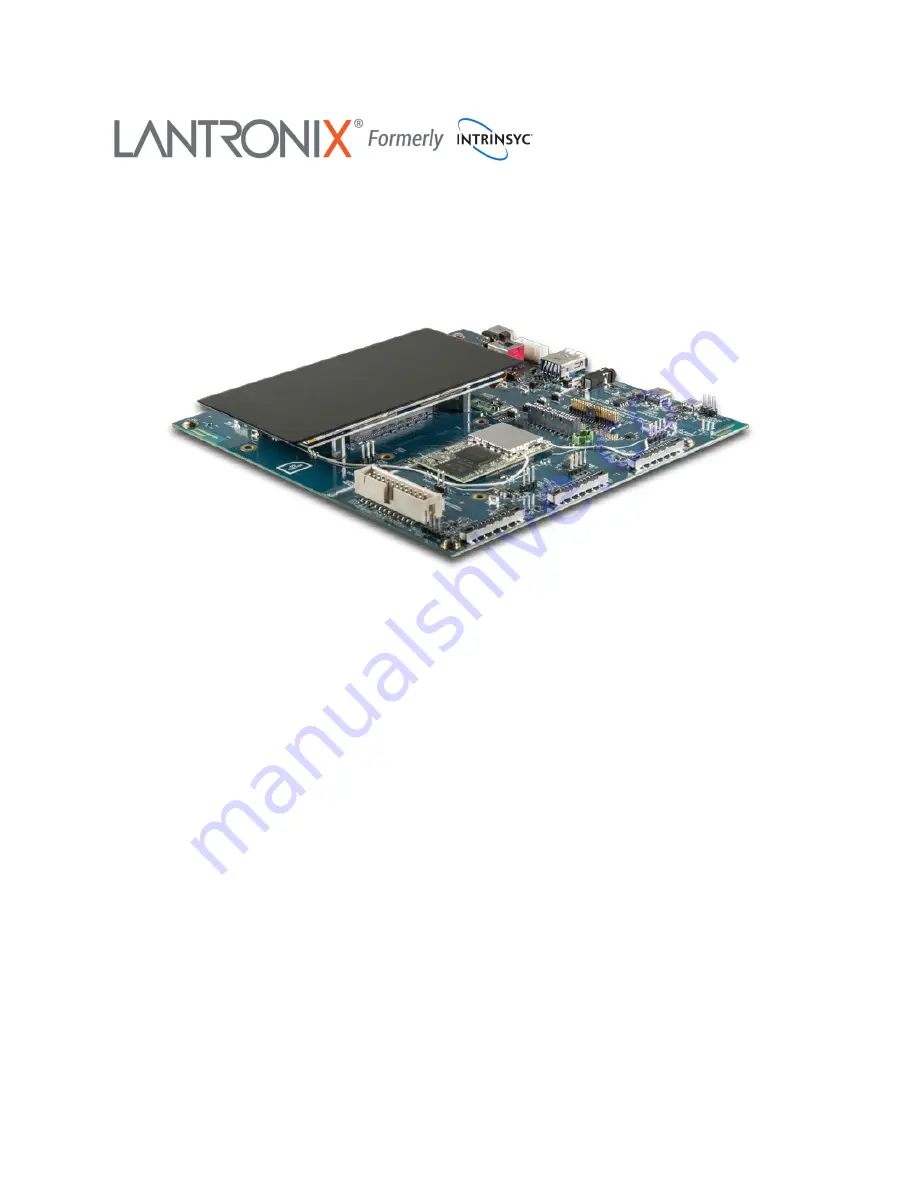
Страница 11: ...e 11 3 4 1 Important Locations The diagram below shows the locations of key components interfaces and controls 2 1 4 3 29 30 34 5 8 9 10 11 12 7 13 14 17 20 16 19 15 37 36 21 22 27 23 26 18 28 32 31 33 38 6 25 35 40 39 41 42 24 Figure 1 Assembled Open Q 865XR SOM Development Kit ...
Страница 12: ... Power Volume Up Volume Down S2401 S2403 S2400 S2402 8 Audio Headset Jack J1700 9 Debug UART Header J1501 10 Audio I O Header J1900 11 USB 3 1 Type C connector for ADB J2200 12 USB Serial Debug Console J1500 13 WLAN BT Channel 0 External Antenna Connector J2601 14 WLAN Channel 1 External Antenna Connector J2600 15 Camera 1 Connector J1000 16 Camera 2 Connector J1100 17 Camera 3 Connector J1200 18 ...
Страница 13: ...f Carrier Board underneath Display Adapter U1600 29 Power Header J700 30 Coin Cell Holder B300 31 Open Q 865XR SOM WLAN BT CH0 Antenna Connector J3700 on SOM 32 Open Q 865XR SOM WLAN CH1 Antenna Connector J3800 on SOM 33 Open Q 865XR SOM 34 On Board Quiet Thermistor RT800 35 SOM Current Sense Probe Header SOM_SYS_PWR J301 36 LEDs BOOT State Blue Green Red DS2403 DS2400 DS2401 DS2402 37 System Conf...
Страница 14: ...ON CONN PM8150L RGB_GRN PM8150L RGB_RED PM8150L RGB_BLU VBATT 3V9 TPS61253 5V BOOST TPS630252 3 3V BUCK RT8077 1 5V BUCK LD39200 1V3 1V1 x3 CAM RP114K281 3V3 2V8 X3 CAM MB_VREG_5P0 MB_VREG_3P3 MB_VREG_1P5 MB_CAM0 1 2_AVDD MB_CAM0 1 2_VCM MB_VREG_1P5 VREG_CAM0 1 2_DVDD VREG_L9C_2P96 USB Type A USB1_VBUS GPIO156 159 LPI MI2S2 MV_VREG_1P8 MB_VREG_3P3 MB_VREG_5P0 DC_IN_12V VREG_WLED MI2S SPEAKER I2S T...
Страница 15: ...ting the development kit serial number 3 5 2 Configuration Switch Settings The default configuration for the system configuration DIP switch S2500 is for all switches to be open or OFF and Header J2500 is open For details about other configurations see section 3 7 2 3 5 3 Powering Up the Development Kit The development kit can be powered up by either using a DC power supply or by connecting a batt...
Страница 16: ...t other external hardware devices to the Open Q 865XR SOM Development Kit Users must ensure that before connecting any hardware device to the development kit that it is compatible with the Open Q 865XR hardware specifications See Figure 1 for position on carrier board Table 2 Carrier Board Features Item Position Description Specification Usage Form Factor Dimensions 170mm x 170mm Mini ITX Form Fac...
Страница 17: ...9 3 pin header 1 8V UART debug header UART debug Micro SD on bottom 22 Micro SD card 4bit Micro SD card support External Storage USB Type C 11 USB 3 1 type C connector For USB debugging and client host mode USB Type A 5 Female Type A Connector USB 3 1 Host interface WLAN Antennas 13 14 2 PCB Antennas Coax connection to SOM WiFi module Coin Cell Holder 30 Coin Cell battery holder provided for PMIC ...
Страница 18: ...tional For WWAN M 2 PCI express cards 3 7 1 SOM Board to Board Connectors 33 The Open Q 865XR SOM connects to the carrier board via two 100 pin and one 120 pin Hirose DF40 connectors which allows essential power rails and signals to be exposed for supporting other peripherals and interfaces on the platform For the list of signals exposed by the SOM see the device specification Ref R 1 3 7 2 Boot C...
Страница 19: ...ols the auto boot of the SOM when power is applied Default configuration is open OFF To enable auto boot of the SOM when power is applied set switch closed ON FORCED_USB_BOOT J2500 For factory mode programming Connected to CPU GPIO132 For Lantronix use only Leave open 3 7 3 Input Power Selection The development kit can be powered using either external DC power supply or by using a battery The inpu...
Страница 20: ...stor on the carrier board For battery powered dev kit set switch to open OFF if thermistor is included on the battery pack Otherwise keep switch closed ON BATTERY ID S301 2 Informs the 865XR SOM whether a valid battery is connected The setting is used as input to enable or disable battery charging For DC power dev kit set switch to closed ON default to disable battery charging For battery power de...
Страница 21: ...BATT_CONN Battery Positive Wire 3 7 4 Current Sense Header J301 35 and J901 39 The SOM Current Sense header J301 can be used to monitor the SOM CB VPH_PWR current consumption on the main SOM_SYS_PWR power rail The VPH Current Sense header J901 can be used to monitor the CB VPH_PWR current consumption on the VPH_PWR power rail The SOM power consumption can be calculated by SOM CB VPH_PWR CB VPH_PWR...
Страница 22: ...r consumption measurements the header is connected to a data acquisition unit Keithley 2701 or similar and the voltages on the SOM_PWR_SENSE_P N pins are captured a few times a second over the test period typically 30 minutes The SOM power consumption is then calculated as where Rsense 5 milliohms 𝑃𝑃 𝑠𝑠𝑠𝑠𝑠𝑠 𝑣𝑣𝑣𝑣ℎ_𝑝𝑝𝑝𝑝𝑝𝑝 𝑉𝑉𝑉𝑉𝑉𝑉𝑚𝑚𝑝𝑝𝑝𝑝𝑟𝑟𝑠𝑠𝑠𝑠𝑠𝑠𝑠𝑠𝑒𝑒𝑁𝑁 𝑉𝑉𝑉𝑉𝑉𝑉𝑚𝑚𝑝𝑝𝑝𝑝𝑟𝑟𝑠𝑠𝑠𝑠𝑠𝑠𝑠𝑠𝑒𝑒𝑃𝑃 𝑉𝑉𝑉𝑉𝑉𝑉𝑚𝑚𝑝𝑝𝑝𝑝𝑟𝑟𝑠𝑠𝑠𝑠𝑠𝑠𝑠𝑠𝑒𝑒...
Страница 23: ...E_P VPH power positive current sense line 2 VPH_PWR_SENSE_N VPH power negative current sense line 3 GND System Ground The SOM power consumption can be calculated by 𝑃𝑃𝑃𝑃𝑃𝑃𝑃𝑃 𝑃𝑃 𝑠𝑠𝑠𝑠𝑠𝑠 𝑣𝑣𝑣𝑣ℎ_𝑝𝑝𝑝𝑝𝑝𝑝 𝑃𝑃𝑃𝑃𝑃𝑃ℎ_𝑝𝑝𝑝𝑝𝑝𝑝 3 7 5 Coin Cell Battery Holder B300 30 The coin cell holder allows the user to use a coin cell for supplying power to the SOM VCOIN power input It is recommended that the Panasonic ML621 s...
Страница 24: ...MB_ELDO_CAM3_VCM_2P85 2 85V Carrier Board LDO for Camera 4 VCM 7 MB_ELDO_CAM1_DVDD_1P1 1 1V Carrier Board LDO for Camera 2 DVDD Camera core 8 VREG_L5F_2P85 2 85V SOM Board power for Camera AVDD 9 MB_ELDO_CAM0_AVDD_2P85 2 85V Carrier Board LDO for Camera 1 AVDD 10 GND System Ground 11 VREG_L3F_1P0 1 0V SOM Board power for Camera 3 DVDD Camera core 12 MB_VREG_3P3 3 3V Carrier Board buck boost power ...
Страница 25: ... 1 for the carrier board locations of the user buttons and LEDs respectively Table 9 Development Kit Buttons 7 Reference Designator User Button Function S2400 Volume Use this button to control or increase the volume S2402 Volume Reset Use this button to control or decrease the volume This button can also be used to reset the board S2401 GP User This is a general purpose user button connected to GP...
Страница 26: ...location of J1500 on the carrier board 3 7 9 Optional Debug UART Header J1501 9 The UART connection used on the Open Q 865XR is a UART header J1501 This is an optional debug header This debug header and J1500 should not be used at the same time The following table describes the pinout of the debug UART header This debug UART is available over USB via the USB to TTL Serial 1 8V cable To get the ser...
Страница 27: ... situated on the north side of carrier board which exposes USB 3 1 host functionality This USB connection is designed to provide up to 1A VBUS current for external devices See item 5 in Figure 1 for the location of J2300 on the carrier board If the user intends to use a M 2 PCIe card on the dev kit that requires a USB connection see 3 7 15 below then the M 2 PCIe USB enable DIP switch S2301 6 must...
Страница 28: ...M Development Kit It can be purchased by contacting sales http www lantronix com about us contact Exposed on the display connector are the following interfaces Two 4 lane MIPI DSI high speed display interfaces LCD backlight control signals I2C bus for touch panel support Additional GPIOs for general purposes available Various power rails for powering the display adapter For details on the signal l...
Страница 29: ...the camera connectors Lantronix offers compatible camera module accessories for the Open Q 865XR SOM Development Kit here https shop intrinsyc com collections accessories Exposed on each camera connector are the following interfaces One 4 lane MIPI CSI high speed camera interface Camera Control Interface CCI I2C bus for camera and actuator control Additional GPIOs for general purposes available Va...
Страница 30: ...See items 18 19 and 20 in Figure 1 for the carrier board locations of the camera option connectors The pinout of the connectors in shown in the table below Table 12 Camera option Connectors pinout Pin No Signal Name Description 1 CAM_FRAME_SYNC Camera connector pin 12 frame sync need wires to other GPIO header 2 CAM_FLASH_TRIG Camera connector pin 18 flash trigger need wires to other GPIO header 3...
Страница 31: ...ies with the PCI Express M 2 card standards Please refer to the document at the following link for more information https www pcisig com specifications pciexpress base mini1 2 Special Notes The optional SIM card socket J2701 25 can be used if the user is connecting a M 2 PCIe card with cellular connection capabilities If the user intends to use a M 2 PCIe card on the dev kit that requires a USB co...
Страница 32: ... this header is shown in the table below Table 13 Digital IO Expansion Header J2100 Pinout Pin No Signal Description Pin No Signal Description 1 No Net No Net 2 VREG_S4A_1P8 SOM LDO Regulator S4A 1 8V 3 GPIO_41_QUP14_FP_S PI_MOSI CPU GPIO41 QUP1 4 4 MB_VREG_3P3 Carrier board switching regulator 3 3V 5 GPIO_40_QUP14_FP_S PI_MISO CPU GPIO40 QUP1 4 6 PM8150L_GP10_PWM PM8150L GPIO10 7 GPIO_43_QUP14_FP...
Страница 33: ...cations See item 21 in Figure 1 for the carrier board location of this header The pinout for this header is shown in the table below Table 14 Sensor Expansion Header J2000 Pinout Pin No Signal Description Pin No Signal Description 1 GPIO_170_SNS_I2C4_SD A GPIO_170 SSC10 SSC4_I2C_SDA 2 GPIO_123_IMU1_INT GPIO123 3 GPIO_171_SNS_I2C4_SC L GPIO_171 SSC11 SSC4_I2C_SCL 4 GPIO_112_IMU2_INT GPIO112 5 GPIO_...
Страница 34: ... the audio input capabilities of WCD9385 for the user See item 27 in Figure 1 for the carrier board location of this header The pinout for this header is shown in the table below Table 15 Audio Inputs Expansion Header Pinout J1800 Pin No Signal Description Pin No Signal Description 1 CDC_IN1_P Codec Input 1 Positive 2 CDC_IN1_N Codec Input 1 Negative 3 CDC_IN6_P Codec Input 6 Positive 4 CDC_IN6_N ...
Страница 35: ...ualcomm Audio Codec WCD9385 28 The Audio Outputs Expansion Header J1801 exposes some of the audio output capabilities of WCD9385 for the user See item 26 in Figure 1 for the carrier board location of this header The pinout for this header is shown in the table below Table 16 Audio Outputs Expansion Header Pinout J1801 Pin No Signal Description Pin No Signal Description 1 CDC_LINE_OUT1_P Codec Line...
Страница 36: ...00 exposes some of these interfaces for the user See item 10 in Figure 1 for the carrier board location of this header The pinout for this header is shown in the table below Table 17 Audio IO Expansion Header Pinout J1900 Pin No Signal Description Pin No Signal Description 1 GPIO_152_LPI_ MI2S1_CLK_R CPU GPIO152 can be configured as LPI_MI2S1_MCLK 2 GND System Ground 3 GPIO_153_LPI_ MI2S1_WS CPU G...
Страница 37: ...1_ R CPU GPIO159 can be configured as LPI_MI2S_DATA1 21 GPIO_149_LPI_ MI2S0_DATA1 CPU GPIO149 can be configured as LPI_MI2S0_DATA1 22 GND System Ground 23 GPIO_150_LPI_ MI2S0_DATA2 CPU GPIO150 can be configured as LPI_MI2S0_DATA2 24 GPIO_4_QUP1_ NFC_I2C_SDA CPU GPIO4 can be configured as QUP1_NFC_I2C_SDA 25 GPIO_151_LPI_ MI2S0_DATA3 CPU GPIO151 can be configured as LPI_MI2S0_DATA3 26 GPIO_5_QUP1_ ...
Страница 38: ...Q 865XR SOM Development Kit WLAN BT functionality is based on Qualcomm QCA6391 chipset It provides WLAN Bluetooth in 2x2 MIMO with two spatial streams IEEE802 11 a b g n ac ax WLAN standards and Bluetooth LE 5 x HS enabling seamless integration of WLAN Bluetooth and low energy technology The QCA6391 chipset is located on the SOM which has U FL coax connectors for channel 0 WLAN BT and channel 1 WL...