background image

15


www.lairdtech.com


Laird Technologies


BTM520/521

Bluetooth

® 

Multimedia Plus Module

CONFIGURING  

THE BTM520/521

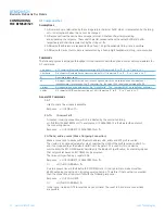
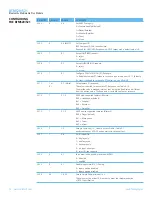
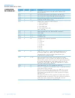
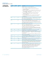
Table 3-1: S-Register List

REGISTER

DEFAULT

RANGE

COMMENT

S0

1

-1..15

Number of RING indication before automatically answering an incoming 
connection. A value of 0 disables autoanswer. If -1, then autoanswer on one 
RING and do NOT send RING/CONNECT response to the host. This emulates a 
serial cable replacement situation 

Setting values >= 0, resets S Register 504 to 0 and <0 forces 504 to 1.

If S0 <> 0 and S100 <> 0 then S0 must be < S100. If a value is entered which 
violates this rule, then ERROR 29 is sent in response.

If S504 =1 then this register will return -1, regardless of the actual value 

stored in non-volatile memory.

S2

0x5E

0x20..0x7E

Escape sequence character. It is not ‘+’ by default as a 

Bluetooth

®

 serial link 

can be used to connect to a mobile phone which exposes an AT command 
set, which will in turn use ‘+’ as default. So if both used ‘+’ there will be 
confusion. 0x5e is the character ‘^’.

S12

100

40..5000

Escape sequence guard time in milliseconds, with a granularity of 20ms. New 
values are rounded down to the nearest 20ms multiple

S100

15

0..15

Number of RING indications before an auto disconnection is initiated. A value 
of 0 disables this feature.
If S0 <> 0 and S100 <> 0 then S0 must be < S100. If a value is entered which 
violates this rule, then ERROR 29 is sent in response.

S101

$1101 

0..$ffff

UUID of default SPP based profile when not specified explicitly in the ATD 

command.

S102

1

1..0x7FF

Defines a set of bits masks for enabling profile servers. Values can be ORed.
0x001 is Serial Port Profile
0x080 is A2DP

0x100 is AVRCP

S103

1

1..7

Boot Mode on cold boot.

S126

?

0 .. 0xFFFF

Primer for changing to Multipoint mode

S127

?

0 .. 0xFFFF

0x100 for At mode
0x200 for Multipoint mode
Other values are reserved

S300

1

0..2

Set A2DP role:

0 is feature not set

1 is A2DP Sink (default)

2 is A2DP Source

S301

1

0..2

Set AVRCP role:

0 is feature disabled

1 is Control (CT) (default)
2 is Target (TG)


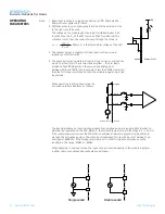
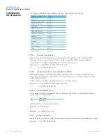
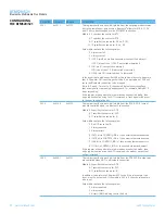
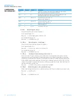
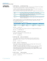
8. ATSn=m        {Set S Register}


  As with modems, the Bluetooth module employs a concept of registers which are used to store  


  parameters, such as escape sequence character, inquiry delay time etc, as listed in detail below.


  The value part ‘m’ can be entered as decimal or hexadecimal. A hexadecimal value is specified via 


  a ‘$’ leading character. For example $1234 is a hexadecimal number.


  When S register values are changed, the changes are not stored in non-volatile memory UNTIL  


  the AT&W command is used. Note that AT&W does not affect S registers 520 to 525 or 1000 


  to 1010 as they are updated in non-volatile memory when the command is received.

Содержание BTM521

Страница 1: ...BTM520 521 DATA MODULE USER MANUAL Innovative Technology for a Connected World www lairdtech com...

Страница 2: ...521 11 References 11 Glossary of Terms 12 AT Command Set 13 Assumptions 13 Commands 13 General AT Commands 13 General Bluetooth Control 24 Hardware Unit Control 30 Bluetooth Profiles 32 Secure Simple...

Страница 3: ...fied so that no further Bluetooth qualification is required For users with more complex applications additional profiles will be available for file transfer object exchange dial up networking messagin...

Страница 4: ...or internal antenna options HSP HFP A2DP and AVRCP audio profiles Future support for OBEX DUN FTP HDP profiles for additional functionality 16 bit stereo codec and microphone input Integrated audio a...

Страница 5: ...supported Bits 8 Parity Odd even none Stop bits 1 or 2 Default Serial parameters 9600 n 8 1 Levels 1 7 3 6V CMOS independent of Vcc Modem Control RTS CTS DTR DSR DCD RI General Purpose Interface I O...

Страница 6: ...A including speaker drive Low Power Sniff Mode Less than 1 5mA Supply Voltage Supply 3 0V 4 2V DC I O 1 7V 3 6V DC Coexistence Compatibility WLAN 802 11 2 3 and 5 wire hardware coexistence schemes sup...

Страница 7: ...16 VDD_PIO VIO supply 17 VDD_IN Main supply 18 GND 19 AUDIO_GND 20 SPKR_B_P Speaker channel B right Note 3 21 SPKR_B_N Speaker channel B right Note 3 22 SPKR_A_P Speaker channel A left Note 3 23 SPKR...

Страница 8: ...ADC Input 10 bit 0 1 5V input range 68 PIO10 DSR Host I O VPADS 69 PIO11 DTR Host I O VPADS 70 AIO0 ADC Input 10 bit 0 1 5V input range 71 PIO9 DCD Host I O VPADS 72 PIO13 SDA Host I O VPADS 73 PIO8...

Страница 9: ...il 0 3 0 25VDD_USB Output Voltage Levels Voh Iout 4mA 0 75VDD_USB VDD_USB Vol Iout 4mA 0 0 125 Logic Levels VIO Input Voltage Levels Min Typ Max Vih 0 625VDD_IO VDD_IO 0 3 Vil 0 3 0 25VDD_IO Output Vo...

Страница 10: ...icrophone should be biased as follows The input impedance on the microphone inputs in microphone mode is typically 6k In order to maintain the regulation on the MIC_BIAS pin the current drawn must be...

Страница 11: ...subsequent power up the device is discoverable or automatically connects The device has a serial interface which can be configured for baud rates from 1200 up to 921600 default setting is 9600 and an...

Страница 12: ...g an analogue digital signal DAC Digital to Analogue Converter DSP Digital Signal Processor DUN Dial Up Network Profile FTP File Transfer Profile GOEP Generic Object Access Exchange Profile GPIO Gener...

Страница 13: ...ng delimited by double quotes E g Hello World The character MUST be supplied as delimiters uuid A 4 character UUID number consisting of ASCII characters 0 to 9 A to F and a to f General AT Commands 1...

Страница 14: ...rned if the R modifier is specified AND a Bluetooth address If both R and L modifiers are specified then an error will be returned Response cr lf CONNECT 123456789012 AE cr lf Or cr lf NO CARRIER cr l...

Страница 15: ...n is initiated A value of 0 disables this feature If S0 0 and S100 0 then S0 must be S100 If a value is entered which violates this rule then ERROR 29 is sent in response S101 1101 0 ffff UUID of defa...

Страница 16: ...r automatic PT Response see Table 3 10 The written value is mapped internal that is why the Read value is different from the written value The Read value is actually sent out as response S312 1 0 15 A...

Страница 17: ...tions or pairing E g CONNECT NO CARRIER RING PAIR etc Suppressing connection based messaged allows the device to be configured in cable replacement mode S505 10 2 120 Minimum delay before abandoning c...

Страница 18: ...defined by S Reg 566 and if deasserted then S Reg 567 S514 10 1 60 Pairing Timeout in seconds This includes the time a host takes to supply the PIN number when PIN messages are indicated S515 0x001F0...

Страница 19: ...connectable or discoverable then GPIO4 will blink This register will not necessarily be effective immediately after changing the value It must be saved to non volatile store using AT W and will opera...

Страница 20: ...ile in command and connected mode then on going back online using the ATO command a fresh signal will be sent to the peer to update the bits S552 0x0122 0x0FFF This register specifies in each 4 bit ni...

Страница 21: ...y ok When Bit 1 is 1 then error responses do not include the error number and instead the error number can be retrieved using ATI12 S560 15 15 120 Disconnect timeout in seconds This timer specifies ho...

Страница 22: ...ad S Register Valid Range This will return the valid range of values for register n For recognised values of n Response cr lf Sn nnnn mmmm cr lf OK cr lf For unrecognised values of n Response cr lf ER...

Страница 23: ...The chipset format I9 0 if not in a connect state and 1 if in a connect state I11 The reason why a NO CARRIER resulted in the most recent attempt at making an outgoing connection Where the response v...

Страница 24: ...cr lf General Bluetooth Control 1 AT BTAn Control Audio Channel Once a Bluetooth connection is active and assuming the peer device is also a Laird Technologies device this command is used to start sto...

Страница 25: ...the non volatile database If the device is not in the database then the response will still be an OK Response cr lf OK cr lf 5 AT BTD Remove All Trusted Devices This command is used to remove all devi...

Страница 26: ...is used to filter inquiry responses When devclass is 2 hexadecimal characters long it forces the inquiry to filter responses to devices that match their major device class code to this value which can...

Страница 27: ...en the pin is written to non volatile memory for future use Specifying an empty string deletes the key from the non volatile memory The string length must be in the range 0 to 8 otherwise an error wil...

Страница 28: ...e receive buffer until a Bluetooth connection is established with the peer device and it then sends the buffer across This means that if the peer device is not in the vicinity and will never be there...

Страница 29: ...e the AT BTK command For a successful pairing the link key is stored in a volatile cache which is overwritten every time a new pairing is initiated using this command The link key can be stored in a n...

Страница 30: ...690 the overall gain dBr must be entered multiplied by 10 If the input value doesn t match a gain table entry the nearest possible value is set The actually set value can be checked by reading back S6...

Страница 31: ...t 15 See Gain Table S690 is affected too Set input overall gain dBr S690 450 215 default 0 See GainTable value must be entered and is returned multiplied by 10 S590 is affected too Increment current o...

Страница 32: ...ted by setting the appropriate Flag in S Register 102 see Table 3 1 After S Register 102 has been written all S Registers must be saved to non volatile memory AT W and subsequently a reset has to be c...

Страница 33: ...0 450 215 Set codec input gain in dBr 10 applies to source default 0 Set A2DP sink supported features bit mask S312 0 15 Bitmask sink supported features Bit 0 Headphone default Bit 1 Speaker Bit 2 Rec...

Страница 34: ...ommand mode S Register 531 is ignored for AVRCP connections 3 1 2 Release AVRCP control connection AT AVH Release AVRCP control connection Response cr lf NO CARRIER 110E cr lf 3 1 3 Send UNIT INFO Req...

Страница 35: ...r lf AVPTC n operation_idhex button_state cr lf after command completion If status n indicates an unsuccessful outcome operation_idhex and button_state are omitted 3 2 AVRCP Target TG This section des...

Страница 36: ...se S305 0 1 default 1 Enable Subunit Info Response S306 0 1 default 1 Configure PASS THROUGH PT Response S310 0 1 1 Enable automatic PT response response type is read from S311 default 0 Host is requi...

Страница 37: ...x0B Favorite menu 0x0C Exit 0x0D 0 0x20 1 0x21 2 0x22 3 0x23 4 0x24 5 0x25 6 0x26 7 0x27 8 0x28 9 0x29 Dot 0x2A Enter 0x2B Clear 0x2C Channel up 0x30 Channel down 0x31 Sound select 0x32 Input select 0...

Страница 38: ...n of AVRCP control connection request CONNECT 0123456789012 AE 110E AVRCP control connection established 0123456789012 bd_addr of peer device A authenticated E encrypted 110E UUID indicating AVRCP NO...

Страница 39: ...1 specification general bonding is defined as the exchange of link keys between two devices with the intention of establishing a connection immediately This is the case if a device wants to connection...

Страница 40: ...e released ATH may be used Please see Table 3 13 3 Production Info String A string with production information can be retrieved by ATI200 Table 3 13 Profile Release Commands Task AT Command Comment Di...

Страница 41: ..._idhex button_state subunit_idhex subunit_typehex Indication of incoming Pass Through command operation_idhex see Table 3 8 button_state 0 pushed 1 released subunit_idhex subunit id subunit_typehex su...

Страница 42: ...ier cannot be specified in ATD command 35 Invalid Major Device Class valid value in range 0x00 to 0x1F inclusive 36 Pairing in progress Command cannot be actioned try again later 37 Invalid Sniff para...

Страница 43: ...E E D 34 RF OUT SIDE VIEW Description 54 pin BT Voice Module 8X6 Flash Size 20 0 x 14 0 x 2 4mm Pitch 1 0mm Dimension Minimum Typical Maximum Notes H A1 A2 A b A 2 4 2 7 A1 0 8 0 9 1 0 A2 1 5 1 7 b 0...

Страница 44: ...R R16 0R 1 2 R25 NF 0R R25 NF 0R 1 2 R2 0R R2 0R 1 2 C33 NF 100u C33 NF 100u R22 NF 0R R22 NF 0R 1 2 J2 3 way 2 5mm audio jack J2 3 way 2 5mm audio jack 1 2 4 3 C3 100u C3 100u 1 2 SW3 NF SW3 NF 1 3 2...

Страница 45: ...GND 3 OUT 4 VCC 5 U4 CONN_SM_54 U4 CONN_SM_54 PIO_15 DTR 1 PIO_5 BT_STATE BT_PRIORITY 2 PCM_IN 3 PCM_OUT 4 PCM_SYNC 5 PCM_CLK 6 VDD_USB 10 VDD_IO 11 MASTER_VIN 12 SPI_CS 14 SPI_MISO 15 SPI_CLK 16 SPI...

Страница 46: ...M1 Mounting Hole R84 10K R84 10K 1 2 R73 110R R73 110R 1 2 R90 0R R90 0R 1 2 L5 BLM18PG221SN1D L5 BLM18PG221SN1D 1 2 FID2 Fiducial FID2 Fiducial D3 Diode_S1A D3 Diode_S1A 1 2 R11 NF 9K1 R11 NF 9K1 1...

Страница 47: ...Plus Module with integrated antenna DVK BTM520 Development Board with BTM520 soldered in place DVK BTM521 Development Board with BTM521 soldered in place General Comments This is a preliminary user ma...

Страница 48: ...ess statutory and implied or by description regarding the information set forth herein Laird Technologies reserves the right to change specifications at any time and without notice Laird Technologies...

Отзывы: