DV-502/503/DVF-3050/3550
8
CIRCUIT DESCRIPTION
Pin No.
Pin Name
I/O
Description
1
BCK
I
Audio data bit clock input.
2
DATA
I
Audio data digital input.
3
LRCK
I
Audio data latch enable input.
4
DGND
-
Digital ground.
5
VDD
-
Digital power supply (+3.3V).
6
VCC
-
Analog power supply (+5V).
7
VOUTL
O
Analog output for L-channel.
8
VOUTR
O
Analog output for R-channel.
9
AGND
-
Analog ground.
10
VCOM
-
Common voltage decoupling.
11
ZEROR
O
Zero flag output for R-channel.
12
ZEROL
O
Zero flag output for L-channel.
13
MD
I
Mode control data input.
14
MC
I
Mode control clock input.
15
ML
I
Mode control latch input.
16
SCK
I
System clock input.
2-2 D/A Converter : PCM1748(IC801)
Pin No.
Pin Name
I/O
Description
38
CLK
I
The system clock input. all other inputs are registered to the SDRAM on
the rising edge of CLK.
37
CKE
-
Controls internal clock signal and when deactivated, the SDRAM will be one
of the states among power down, suspend or self refresh.
19
CS
-
Enables or disables all inputs except CLK, CKE, and DQM.
20,21
BA0,BA1
-
Selects bank to be activated during RAS activity.
Selects bank to be read/written during CAS activity.
23~26
A0~A11
-
Row address : RA0~RA11, Column address : CA0~CA7
29~35
Auto-precharge flag : A10
18
WE,CAS,RAS
-
WE, CAS and RAS define the operation.
15,39
LDQM,UDQM
I/O Controls output buffers in read mode and masks input data in write mode.
2,4,5,7,8,
10,11,13,42
DQ0~DQ15
I/O Multiplexed data input/output pin.
44 45,47,48
50,51,53
9
VDD/VSS
-
Power supply for internal circuits and input buffers.
10
VDDQ/VSSQ
-
Power supply for output buffers.
11
NC
-
Unused
2-3 64 Bit SDRAM : KS641632D(IC301)
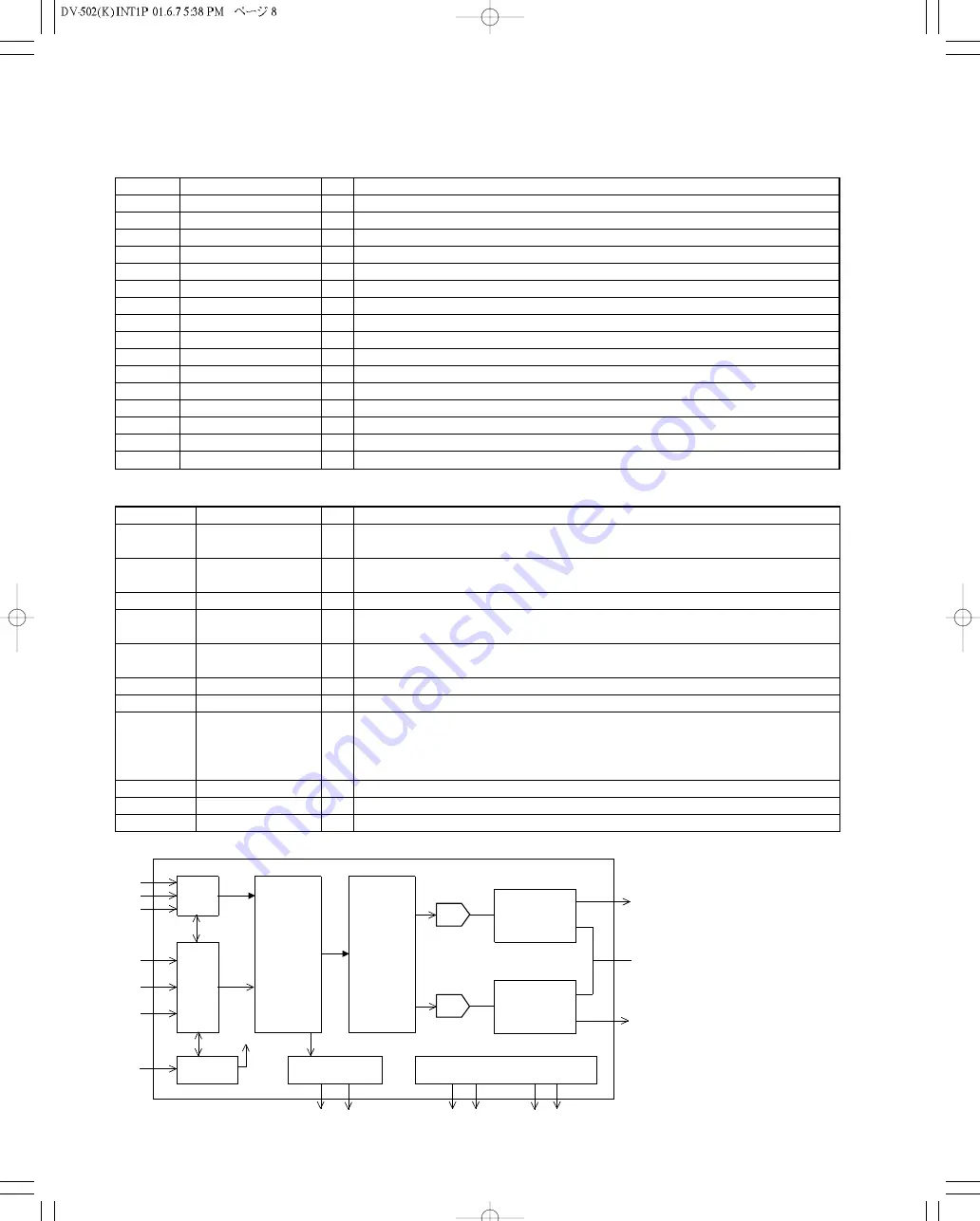
Block Diagram for D/A Converter
BCK
Serial
LRCK
Input
Vout L
DATA
I/F
Output Amp and
Low-pass Filter
8X
Oversampling
Enhanced
Digital Filter
Multi-level
Vcom
ML
Function
with
Delta-Sigma
Function
Modulator
MC
Control
Controller
Output Amp and
MDI
I/F
Low-pass Filter
Vout R
System Clock
SCK
System
Clock
Manager
\Zero Detect
Power Supply
ZERO L
ZERO R
VDD
DGND
VCC
AGND
DAC
DAC


