CD-4900M/DPF-J9030
4
CIRCUIT DESCRIPTION
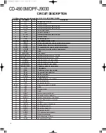
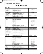
Pin No.
Pin Name
I/O
Description
1
A2
O
Address bus of SRAM.
2
NC
-
No connection.
3
S3-SW
I
Mechanism address detector switch.
4
S2-SW
I
Mechanism address detector switch.
5
RD
O
SRAM read strobe.
6
WR
O
SRAM write strobe
7
S1-SW
I
Mechanism address detector switch.
8
ASTB
O
No connection.
9
VDD
-
Power 5V).
10
+5VPUL
O
Disc sensor ON/OFF. L:on
11
RTRN
I
TX permission data to remote control microprocessor.
12
RWR
I
Reading data of remote control microprocessor.
13
RWRR
O
TX request data to remote control microprocessor.
14~21
L-D7-D0
O
Data output to remote control microprocessor.
22
TEST
-
GND.
23
DISC-SW
I
Disc sensor.
24
ROTARY-CW
O
Mechanism rotary motor(+). H:CCW
25
ROTRAY-CCW
O
Mechanism rotary motor(-). H:CW
26
LOADM+1
O
Loading motor(+) for main pickup.
27
LOADM-1
O
Loading motor(-) for main pickup.
28
LOAD-SW1
I
Loading switch for main pickup.
29
UNLOAD-SW1
I
Unloading switch for main pickup.
30
CS
O
Chip selector
31
MON
O
Control port of poor focus works.
32
SCLK
O
Sens serial data read clock.
33
SENS
I
SENS signal input.
34
CLOCK
O
Serial data clock.
35
XLAT
O
CXD2587Q latch. H
î
L:latch
36
DATA
O
Serial data output.
37
VDD
-
Power 5V).
38,39
X1,2
-
Main system clock(12.5MHz).
40
VSS
-
GND.
41
XT2
-
No connection.
42
XT1
I
GND.
43
RESET
I
System reset signal input.
44
SCOR
I
Sub code synchro detection.
45
MUTEG
O
Muting control output. H:muting on.
46
STB2
O
Strobe signal output to dot driver.
47
ICRESET
O
IC reset.
48
SYSM
O
Analog muting. L: Muting on.
49
SDATA
I/O
Serial data signal I/O.
50
SBUSY
I/O
Serial busy signal I/O.
51
AVDD
-
Power 5V).
52
AVREF
-
A/D reference power supply.
53
A/D0
I
Model discrimination.
54
8/16
I
8/16 bit selector. H:16bit.
55
JOG2
I
Encoder signal A input.
1-2 Microprocessor pin description (X32, IC8): UPD784217GF502


