


PCIe/PXIe-5211 |
| 24
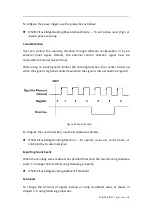
Please refer to chapter 4.5.3 for more information about timebase.
Terminals
To change the terminal of signals instead of using its default value shown in chapter
2.6, use following properties:
JY5211CITask.PulseMeas.InputTerminal – Signal-to-measure input terminal.
JY5211CITask.PulseMeas.Timebase.External.Terminal – External timebase input
terminal.
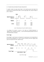
Learn by Examples 4.3.2
Connect the signal source’s positive terminal Ch1 to PCIe/PXIe-5211 counter0’s
pulse measure source (CTR0_Gate, Pin#31), negative terminal to the ground
(GND, Pin#32) as shown in
Table 2-15 Pin Defination
. (CTR0_Gate, GND) consists
of a pulse measure counter input.
Set the signal source Ch1’s output to squarewave signal (f=1Hz, Duty Cycle=50%,
�
�
=3.3v,
�
�
=0v).
Single Mode
Open
Counter Input-->Winform CI Single Pulse
, set the following numbers as
shown:
Figure 17 Pulse Measure In Single Mode
The table in the sample program is a connection diagram for your convenience.
Содержание PCIe-5211
Страница 1: ...User Manual Version Revision Date V1 6 2 Oct 09 2021 PCIe PXIe 5211 Counter Timer Module User Manual...
Страница 9: ...PCIe PXIe 5211 jytek com 5 2 2 Digital IO Specifications Table 1 Digital IO Specifications...
Страница 10: ...PCIe PXIe 5211 jytek com 6 2 3 Counter Timer Specifications Table 2 Counter Timer Specifications...
Страница 11: ...PCIe PXIe 5211 jytek com 7 2 4 Other Specifications Table 3 Other Specifications...
Страница 12: ...PCIe PXIe 5211 jytek com 8 2 5 Front Panel and Pin Definition Figure 3 Front Pannel...
Страница 13: ...PCIe PXIe 5211 jytek com 9 Table 4 Pin Defination...
Страница 36: ...PCIe PXIe 5211 jytek com 32 Figure 24 Frequency Measure Values In Single Mode...


