

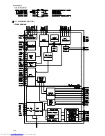


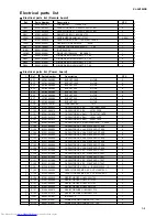
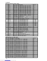
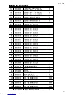
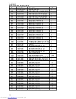

1-10
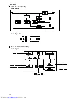
XL-SV205GD
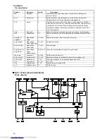
U2: C16256 (4MB DRAM)
Block diagram
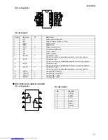
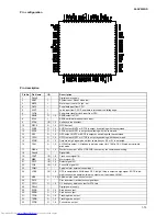
Pin configuration
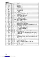
Pin description
Pin No.
Pin Name
Type
Description
16~19,22~26
A0-A8
Input
Address input
14
RAS
Input
Row address
strobe
28
CASH
Input
Column address
strobe/Upper
byte control
29
CASL
Input
Column address
strobe/lower
byte control
13
WE
Input
Write enable
27
OE
Input
Output enable
2~5,6~10,
I/O1 - I/O16
Input/Output Data input/
31~34,36~39
output
1,6,20
V c c
Supply
Power, 5V
21, 35, 40
V s s
Ground
Ground
11,12,15,30
NC
-
No connect
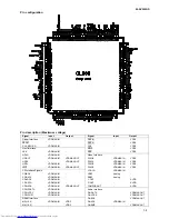
Содержание XL-SV205GD
Страница 12: ...1 12 XL SV205GD U7 CXD3068Q CD DSP Block diagram Pin description ...
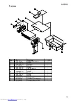
Страница 19: ...3 2 XL SV205GD Exploded view diagram Main unit exploded view diagram ...
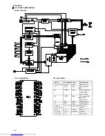
Страница 28: ...2 1 XL SV205GD Wiring diagram ...
Страница 29: ...2 2 XL SV205GD Block diagram ...
Страница 30: ...XL SV205GD 2 3 Schematic Diagrams MIC AMP Power Key FLD Circuit ...
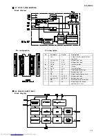
Страница 34: ...XL SV205GD 2 7 Printed Circuit Boards Power supply AC selector AC switch board Top view ...
Страница 35: ...XL SV205GD 2 8 MPEG Servo Output Board Fig 1 ...
Страница 36: ...XL SV205GD 2 9 MPEG Servo Output Board Fig 2 Fig 3 ...