RX-DP10VBK/RX-DP10VSL
RX-DP10RSL
1-21
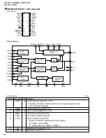
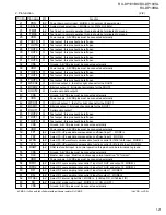
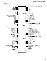
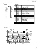
2. Pin function
(2/2)
Pin name
PDN
CKSLN
TMD1
TMD0
VDD
TOUTD
TOUTA
TOUT9
TOUT8
TOUT7
TOUT6
VSS
VDD
TOUT5
TOUT4
TOUT3
WCKO2
BCKO2
DOUT2
VSS
VDD
WCKO1
BCKO1
DOUT1
TOUT2
TOUT1
TOUT0
VSS
VDD
FP1
FP2
WSN
WS
RAMT
VSS
CLK
VDD
DFR1
DFR2
DF1
DF2
DFSEL
SH
VSS
I/O
lp2
lp2
lp2
lp2
-
O
O
O
O
O
O
-
-
O
O
O
O
O
O
-
-
O
O
O
O
O
O
-
-
lp2
lp2
lp2
lp2
lp2
-
l
-
lp2
lp2
lp2
lp2
lp2
lp2
-
Function
Power down control input ; MODE=L, (L=normal, H=power down)
System clock select input ; MODE=L, (L=512fs, H=384fs)
Test input ; in normal operation this pin should be terminated to ground
Test input ; in normal operation this pin should be terminated to ground
Power supply ; All VDD pins must be connected externally
Test output ; this pin should be left open
Test output ; this pin should be left open
Test output ; this pin should be left open
Test output ; this pin should be left open
Test output ; this pin should be left open
Test output ; this pin should be left open
Ground ; All VSS pins must be connected externally
Power supply ; All VDD pins must be connected externally
Test output ; this pin should be left open
Test output ; this pin should be left open
Test output ; this pin should be left open
L/R clock output 2 ; the left or right channel for the DOUT2
Bit clock output 2 ; bit clock of serial data for the DOUT2
Serial audio data output 2
Ground ; All VSS pins must be connected externally
Power supply ; All VDD pins must be connected externally
L/R clock output 1 ; the left or right channel for the DOUT 1
Bit clock output 1; bit clock of serial data for the DOUT1
Serial audio output 1
Test output ; this pin should be left open
Test output ; this pin should be left open
Test output ; this pin should be left open
Ground ; All VSS pins must be connected externally
Power supply ; All VDD pins must be connected externally
Select FS-UP peak data compensation coefficient input 1 ; MODE=L
Select FS-UP peak data compensation coefficient input 2 ; MODE=L
Select FS-UP waveform compensation function control for 16fd to 9fd input ; MODE=L
Select FS-UP waveform compensation function control for 8fd to 2fd input ; MODE=L
RAM test control input ; in normal operation this pin should be terminated to ground
Ground ; All VSS pins must be connected externally
Master clock input ; Must run continuously normal operation, "5V tolerant"
Power supply ; All VDD pins must be connected externally
Select DF over sampling rate control 1 input for FS-UP and output 2 ; MODE=L
Select DF over sampling rate control 2 input for FS-UP and output 2 ; MODE=L
Select DF over sampling rate control 1 input for output 1 ; MODE=L
Select DF over sampling rate control 2 input for output 1 ; MODE=L
Select DF internal digital fitter ; MODE=L, (L=84tap FIR, H=169tap FIR)
Select SH mode control input ; MODE=L, (L=ON, H=OFF)
Ground ; All VSS pins must be connected externally
Pin No.
21
22
23
24
25
26
27
28
29
30
31
32
33
34
35
36
37
38
39
40
41
42
43
44
45
46
47
48
49
50
51
52
53
54
55
56
57
58
59
60
61
62
63
64
l=CMOS, l1=Schmitt, lp2=Schmitt with pull-down resistor, O=CMOS
(H=VDD, L=VSS)
Содержание RX-DP10RSL
Страница 61: ...RX DP10VBK RX DP10VSL RX DP10RSL 3 2 M E M O ...
Страница 94: ...RX DP10VBK BX DP10VSL RX DP10RSL 3 35 M E M O ...
Страница 97: ...RX DP10VBK RX DP10VSL RX DP10RSL 3 38 M E M O ...
Страница 99: ...RX DP10VBK RX DP10VSL RX DP10RSL 3 40 M E M O ...
Страница 130: ...RX DP10VBK BX DP10VSL RX DP10RSL 3 71 M E M O ...


