background image

(No.YA712<Rev.002>)1-13

4.6

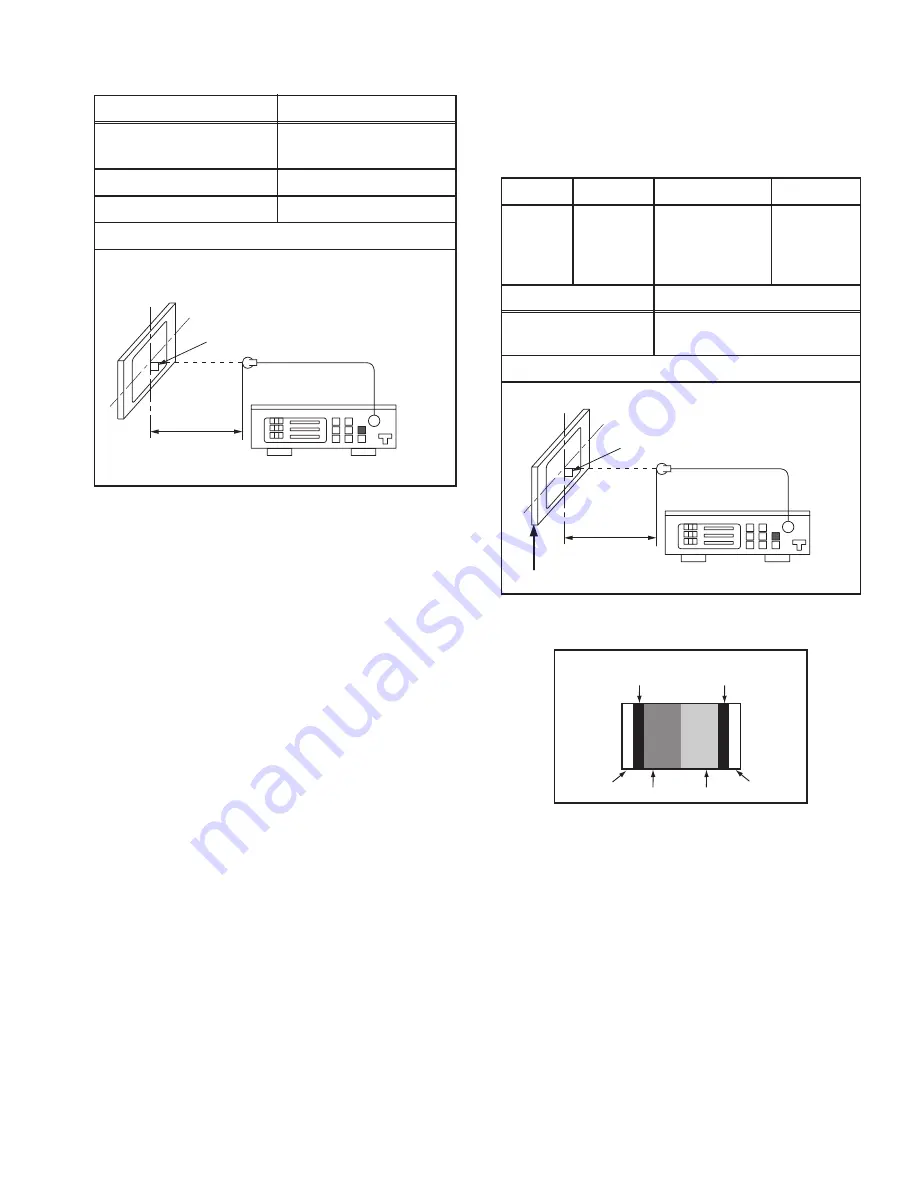
VCOM ADJUSTMENT

(1) Operate the unit for more than 20 minutes.
(2) Set the color analyzer and bring the optical receptor to the

center on the LCD-Panel surface after zero point calibra-
tion as shown above. 

Note:

 The optical receptor must be

set perpendicularly to the LCD Panel surface.

(3) Enter the Service mode. 
(4) Press [3] button on the service remote control unit.
(5) Press [CHANNEL UP/DOWN] buttons on the service re-

mote control unit so that the color analyzer value becomes
minimum.

4.7

WHITE BALANCE ADJUSTMENT

The white balance adjustment should be performed when
replacing the LCD Panel or Digital PWB.
Purpose:

 To mix red, green and blue beams correctly for pure

white. 

Symptom of Misadjustment: 

White becomes bluish or reddish.

(1) Operate the unit for more than 20 minutes.
(2) Input the White Raster(70%=70IRE, 40%=40IRE).

(3) Set the color analyzer to the CHROMA mode and bring the

optical receptor to the center on the LCD-Panel surface af-
ter zero point calibration as shown above.

Note:

 The optical receptor must be set perpendicularly to

the LCD Panel surface.

(4) Enter the Service mode. Press [VOLUME DOWN] button

on the service remote control unit and select "C/D" mode.

(5)

[CUTOFF]

Press [1] button to select “COR” for Red Cutoff adjustment.
Press [3] button to select “COB” for Blue Cutoff adjustment.

[DRIVE]

Press [4] button to select “DR” for Red Drive adjustment.
Press [6] button to select “DB” for Blue Drive adjustment.

(6) In each color mode, press [CHANNEL UP/DOWN] buttons

to adjust the values of color.

(7) Adjust Cutoff and Drive so that the color temperature be-

comes 12000

°

K (x= 0.272 / y= 0.278 ±0.005).

Test Point

Adj. Point

Screen

  [CHANNEL UP/DOWN ] 

buttons

M. EQ.

Spec.

Color analyzer

See below

Figure

Color Analyzer

To avoid interference from ambinent 
light, this adjustment should be 
performed in a dark room.

L = 3 cm

Perpendicularity

Test Point Adj. Point

Mode

Input

Screen

[VOLUME 

DOWN]

button

[VIDEO1]

C/D

White Raster 

(APL 70%)

or

(APL 40%)

M. EQ.

Spec.

Pattern Generator, 

Color analyzer

x= 0.272 ± 0.005
y= 0.278 ± 0.005

Figure

Color Analyzer

L = 3 cm

Perpendicularity

INPUT: WHITE 70%, 40%

To avoid interference from ambinent 
light, this adjustment should be 
performed in a dark room.

40%=40IRE

70%=70IRE

100IRE

100IRE

0IRE

0IRE

INPUT SIGNAL

Low

Light

Hight

Light

Содержание LT-32A200/AK

Страница 1: ...NTS 1 PRECAUTION 1 3 2 SPECIFIC SERVICE INSTRUCTIONS 1 4 3 DISASSEMBLY 1 8 4 ADJUSTMENT 1 12 5 TROUBLESHOOTING 1 15 MODEL NO RATING LABEL REAR AK VERSION LT 32A200 MODEL NAME There may be multiple versions of this TV model The TV version is identified by the letters next to the model number on the TV s Rating See illustration Use the service manual that matches the version of the TV HIGH DEFINITIO...

Страница 2: ...alog 3 58 MHz LCD Panel 32 class 31 5 Diagonal wide aspect 16 9 Display Pixels Horizontal 1366 dots Vertical 768 dots W XGA Audio Power Output 10 W 10 W Speaker 1 61 2 79 oval type 2 Antenna Terminal VHF UHF ATSC DIGITAL CABLE IN F type connector 75Ω unbalanced coaxial 1 Video Audio Input VIDEO S Video Mini DIN 4 pin 1 Y 1 V p p Positive Negative sync 75 Ω C 0 286V p p Burst signal 75 Ω Video 1 V ...

Страница 3: ...onents that indicate evidence of overheating should be replaced Always use the manufacturer s replacement components 6 Isolation Check Safety for Electrical Shock Hazard After re assembling the product always perform an isolation check on the exposed metal parts of the cabinet antenna terminals video audio input and output terminals Control knobs metal cabinet screw heads earphone jack control sha...

Страница 4: ...mix different parts number s Trans Inverter 2 2 STANDARD NOTES FOR SERVICING 2 2 1 CIRCUIT BOARD INDICATIONS 1 The output pin of the 3 pin Regulator ICs is indicated as shown 2 For other ICs pin 1 and every fifth pin are indicated as shown 3 The 1st pin of every male connector is indicated as shown 2 2 2 PB LEAD FREE SOLDER Pb free mark will be found on PCBs which use Pb free solder Refer to figur...

Страница 5: ...round the flat pack IC to protect other parts from damage Fig 2 2 3 The flat pack IC on the PWB is affixed with glue so be careful not to break or damage the foil of each pin or the solder lands under the IC when removing it Fig 2 2 WITH SOLDERING IRON 1 Using desoldering braid remove the solder from all pins of the flat pack IC When you use solder flux which is applied to all pins of the flat pac...

Страница 6: ...ers Fig 2 6 NOTE When using a soldering iron care must be taken to ensure that the flat pack IC is not being held by glue When the flat pack IC is removed from the PWB handle it gently because it may be damaged if force is applied Fig 2 5 Fig 2 6 2 2 3 2 INSTALLATION 1 Using desoldering braid remove the solder from the foil of each pin of the flat pack IC on the PWB so you can install a replacemen...

Страница 7: ...y grounded to remove any static electricity that may be charged on the body 2 2 4 2 Ground for Workbench Be sure to place a conductive sheet or copper plate with proper grounding 1MΩ on the workbench or other surface where the semi conductors are to be placed Because the static electricity charge on clothing will not escape through the body grounding band be careful to avoid contacting semi conduc...

Страница 8: ... Tabs L 2 5 Refer to the following Reference Notes in the Table 1 Stand Assembly 2 Rear Cabinet 9 Speaker s 8 Speaker Holder L R 3 Inverter CBA 4 Jack CBA 6 Jack Holder 7 Digital Main CBA Unit 5 Power Supply CBA 13 LCD Module Assembly 14 Front Cabinet 11 IR Sensor CBA 10 Junction CBA 12 Function CBA Step Loc No Part Removal Fig No Remove Unhook Unlock Release Unplug Unclamp Desolder Note 1 Stand A...

Страница 9: ... No YA712 Rev 002 1 9 2 Rear Cabinet S 1 1 Stand Assembly S 2 S 4 S 2 S 3 S 2 S 2 S 4 S 4 Fig D1 ...

Страница 10: ...1 10 No YA712 Rev 002 S 5 S 5 4 Jack CBA 6 Jack Holder 5 Power Supply CBA 7 Digital Main CBA Unit 3 Inverter CBA S 6 S 7 S 8 S 9 S 9 Shield Box S 10 S 11 S 7 S 7 Fig D2 ...

Страница 11: ...A712 Rev 002 1 11 S 14 S 13 S 12 Hook S 15 13 LCD Module Assembly 11 IR Sensor CBA 12 Function CBA 8 Speaker Holder R 8 Speaker Holder L 10 Junction CBA 9 Speaker 14 Front Cabinet S 12 Hook 9 Speaker Fig D3 ...

Страница 12: ...tached remote control unit as shown in Fig 1 4 4 HOW TO SET UP THE SERVICE MODE Service mode 1 Use the service remote control unit 2 Turn the power on 3 Press the service button on the service remote control unit The following screen appears 4 5 PURITY CHECK MODE This mode cycles through full screen displays of red green blue and white to check for non active pixels 1 Enter the Service mode 2 Each...

Страница 13: ...l receptor must be set perpendicularly to the LCD Panel surface 4 Enter the Service mode Press VOLUME DOWN button on the service remote control unit and select C D mode 5 CUTOFF Press 1 button to select COR for Red Cutoff adjustment Press 3 button to select COB for Blue Cutoff adjustment DRIVE Press 4 button to select DR for Red Drive adjustment Press 6 button to select DB for Blue Drive adjustmen...

Страница 14: ...o the USB port as shown below 3 Plug the AC cord in the wall outlet and turn the power on 4 The update will start and the following will appear on the screen NOTE If the above screen isn t displayed repeat from step 1 The appearance shown in 1 is described as follows 5 When the firmware update is completed the following will appear on the screen Unplug the AC cord and kindly remove the USB memory ...

Страница 15: ...tifying circuit of secondary side and service it if defective After servicing replace the fuse When the output voltage fluctuates FLOW CHART NO 3 Does the photocoupler circuit on the secondary side operate normally No Yes Check IC601 D652 Q631 and their periphery circuit and service it if defective When buzz sound can be heard in the vicinity of power circuit FLOW CHART NO 4 Check if there is any ...

Страница 16: ...Q209 Yes Replace Q501 Is approximately 16V voltage supplied to the base of Q501 Yes No Check Q207 Q208 D203 D204 D211 and their periphery circuit and service it if defective No INV 16V is not output FLOW CHART NO 8 Is approximately 19V voltage supplied to the collector of Q501 Yes Check C631 D631 D635 and their periphery circuit and service it if defective Check C631 D631 D635 and their periphery ...

Страница 17: ...f Q641 and the base of Q643 No Yes Yes Check D645 and their periphery circuit and service it if defective No Replace Q641 and Q643 P ON 5V TUNER 5V is not output LCD 16V is outputted normally FLOW CHART NO 11 Is approximately 6 7V voltage supplied to the collector of Q640 Is approximately 6V voltage supplied to the base of Q641 and the base of Q643 Q640 No Yes Yes Check D645 and their periphery ci...

Страница 18: ... base of Q642 Is approximately 5V voltage supplied to Pin 1 of IC631 No Yes Yes Yes Check D670 and their periphery circuit and service it if defective No Check Q635 D659 and their periphery circuit and service it if defective See FLOW CHART No 5 See FLOW CHART No 12 No No AL 3 3V is not output FLOW CHART NO 16 Is approximately 34V voltage supplied to the collector of Q635 Yes Replace IC631 Replace...

Страница 19: ...it Yes Replace Digital Main PWB Unit When pressing each switches SW101A SW103A SW107A do the voltage of Pin 29 of CN302 and Pin 2 of CN303 increase Yes The key operation is not functioning FLOW CHART NO 1 Are the contact point and installation state of the key switches SW101A SW103A SW107A normal Re install the switches SW101A SW103A SW107A correctly or replace the poor switch Check the switches S...

Страница 20: ...r input FLOW CHART NO 4 Are the DIF signal inputted to the Pin 26 28 of CN302 Yes Replace Digital Main PWB Unit or LCD M odule Assembly Replace Digital Main PWB Unit or LCD Module Assembly Pin 6 S VIDEO C Pin 8 S VIDEO Y Picture does not appear normally Y Pb Pr input FLOW CHART NO 6 Are the video signal inputted to the Pin 15 17 19 of CN302 Check the line between Pin 15 17 19 of CN302 and input te...

Страница 21: ...R signals outputted to the Pin 1 2 of CN801 and CN802 Are the audio L R signals outputted to the audio output terminal Check IC801 and their periphery circuit and service it if defective CN802 SP L CN801 SP R JK871 AUDIO L OUT JK872 AUDIO R OUT No Yes Are the audio L R signals inputted to each pin of CN301 Replace Digital Main PWB Unit Check the line between Pin 6 8 of CN301 and Pin 1 44 of IC801 ...

Страница 22: ...e audio L R signals inputted to the Pin 3 5 of IC871 Yes Yes No No Are the audio L R signals outputted to the Pin 1 2 of CN801 and CN802 Are the audio L R signals outputted to the audio output terminal Check IC801 and their periphery circuit and service it if defective CN802 SP L CN801 SP R JK871 AUDIO L OUT JK872 AUDIO R OUT No Yes Check the line between Pin 6 8 of CN301 and Pin 1 44 of IC801 and...

Страница 23: ...utted to the Pin 3 5 of IC871 Yes Yes No No Are the audio L R signals outputted to the Pin 1 2 of CN801 and CN802 Are the audio L R signals outputted to the audio output terminal Check IC801 and their periphery circuit and service it if defective CN802 SP L CN801 SP R JK871 AUDIO L OUT JK872 AUDIO R OUT No Yes Check the line between Pin 6 8 of CN301 and Pin 1 44 of IC801 and service it if defectiv...

Страница 24: ... No YA712 Rev 002 VSE Printed in Japan Victor Company of Japan Limited Display Division 12 3 chome Moriya cho Kanagawa ku Yokohama city Kanagawa prefecture 221 8528 Japan ...

Отзывы: