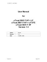
background image

KS-FX925R

1-25

VDD1

VDD2

INH

OSC

CLOCK

GENERATOR

COMON
DRIVER

SEGMENT DRIVER

SHIFT REGISTOR

ADDRESS

DETECTOR

VSS

VDD

DI

CL

CE

S5

S4/P4

S3/P3

S2/P2

S1/P1

S68

S67

COM1

COM2

COM3

LC75873NW (IC601) : LCD driver

1.Pin layout

3.Pin function

2.Block diagram

60    41

1       20

40

21

61

80

Pin No.

Pin name

Description

I/O

I/O

79,80
1,2,3
to 66

S1/P1 TO S4/P4
S5 to S68

COM1
COM2
COM3

Segment outouts for displaying the display data 
transferred by serial data input.
The S1/P1 to S4/P4 pins can be used as general-
purpose output ports under serial data control.

Common driver outputs.
The frame frequency f0 is given by :
f0 = (FOSC/384)Hz.

Oscillator connection 
An oscillator circuit is formed by connecting an 
external resistor and capacitor to this pin.

Serial data transfer inputs.
Connected to the controller.
CE:Chip enable
CL:Synchronization clock
DI:Transfer data

Display off control input
 INH= "L"(VSS)        Display forced off

Used for applying the LCD drive 2/3 bias voltage 
externally. Must be connected to VDD2 when a 
1/2 bias drive scheme is used.

Used for applying the LCD drive 1/3 bias voltage 
externally. Must be connected to VDD1 when a 
1/2 bias drive scheme is used.

Power supply connection.
Provide a voltage of between 3.0 and 6.0V.

Power supply connection. Connect to ground.

S1/P1 to S4/P4 = "L"
(These pins are forcibly set to the 
segment output port function and held
at the low level.)
S5 to S68 = "L"
COM1 to COM3"L"

67
78
69

74

OSC

CE
CL
DI

76 
77 
78

75

INH

VDD1

VDD2

VDD

VSS

71

72

70

73

 INH = "H"(HDD)       Display on
However, serial data transfer is possible when
the display is forced off by this pin.   

O

O

I

I

I

-

-

I
I
I

Содержание KS-FX925R

Страница 1: ... COPYRIGHT 2002 VICTOR COMPANY OF JAPAN LTD KS FX925R KS FX925R Contents Safety precaution Disassembly method Adjustment method Description of major ICs 1 2 1 3 1 11 1 15 26 Area Suffix EE Russian Federation TAPE DAB EQ SOUND VOL VOL SOURCE R F U D ATT ...

Страница 2: ...KS FX925R 1 2 Burrs formed during molding may be left over on some parts of the chassis Therefore pay attention to such burrs in the case of preforming repair of this system Safety precaution ...

Страница 3: ... 2 3 When disengaging the joint c using a screwdriver do not damage or break the board CAUTION Prior to performing the following procedure remove the bottom cover Remove the two screws A attaching the front chassis Remove the two screws B on each side of the body Release the two joints d and the two joints e on the sides remove the front chassis toward the front 1 2 3 Removing the front chassis Se...

Страница 4: ...left side of the body and remove the heat sink 1 Removing the heat sink See Fig 6 Prior to performing the following procedure remove the front chassis the heat sink bottom cover and the rear panel Remove the two screws F attaching the main amplifier board assembly on the top cover Disconnect connector CP401 on the main amplifier board assembly from the cassette mechanism assembly 1 2 Removing the ...

Страница 5: ...CD key control switch board See Fig 10 to 12 Prior to performing the following procedure remove the front panel assembly Remove the four screws H attaching the rear cover on the back of the front panel assembly Unjoint the nine joints f with the front panel and the rear cover Remove the control switch board on the back of the front panel 1 2 3 Cassette mechanism assembly G G Top cover Fig 9 H H H ...

Страница 6: ...sette guide See Fig 3 Remove the screw B on the upper side Unsolder the wires on the under side of the head board if necessary 1 Removing the head board See Fig 4 Prior to performing the following procedures turn the mode gear on the bottom of the body until the respective part comes to the EJECT position Refer to Fig 1 REFERENCE When reassembling twist the wires by turning the head board twice re...

Страница 7: ...ll out the cassette catch from the cassette hanger assembly 1 2 3 4 5 Removing the cassette hanger assembly cassette holder See Fig 6 to 9 Remove the E washer attaching the load arm Move the load arm in the direction of the arrow and release the joint e on the cassette catch 1 2 Removing the load arm See Fig 5 Fig 5 Fig 6 Fig 7 Fig 9 Fig 8 Load arm E washer Joint e Cassette holder assembly Cassett...

Страница 8: ...y See Fig 10 to 12 When reassembling make sure that the boss n of the main chassis is set in the notch of the load rack under the side bracket assembly Do not reattach the load rack on the boss n CAUTION After reattaching the side bracket assembly confirm operation CAUTION Fig 11 Fig 12 Fig 10 C Side bracket assembly Side bracket assembly Joint l Joint m Side bracket assembly Boss n Load rack Boss...

Страница 9: ...assis Remove the rack link 1 2 Removing the slide chassis assembly See Fig 16 and 17 When reassembling first reattach the rack link and next fit the boss p and hook q of the slide chassis assembly to the hole of the main chassis and engage the two joints o CAUTION It is not necessary to remove the head and the tape guide REFERENCE Fig 13 Fig 17 Fig 14 Fig 15 Fig 16 Polywasher Polywasher Pinch arm ...

Страница 10: ...mbly F R See Fig 20 and 21 When reattaching the pinch arm spring set both end of it to the pinch spring arm remarked r CAUTION When reattaching the head set the wires into the groove of the tape guide Fig 18 CAUTION It is not necessary to remove the slide chassis assembly REFERENCE It is not necessary to remove the slide chassis assembly REFERENCE Fig 19 Fig 21 Fig 18 Fig 20 D Slide chassis assemb...

Страница 11: ...ttaching the reel board Move the reel board in the direction of the arrow to release the joint u Unsolder the wires if necessary 1 2 3 Removing the reel board See Fig 25 and 26 When reattaching confirm operation of the MODE switch and the ST BY switch The mode position between EJECT and ST BY is optimum for reattaching Connect the card wire extending from the reel board to the FFC pad before reatt...

Страница 12: ...ion of the arrow to release the two joints w 1 2 3 4 Removing the gear base arm gear base link assembly See Fig 27 to 29 Push each joint hook x of the FFC pad and remove toward the bottom 1 Removing the FFC pad See Fig 27 and 29 When reattaching the gear base arm make sure that the boss on the gear base assembly is inside the gear base spring REFERENCE Fig 27 Fig 28 Fig 29 FFC pad Gear base link a...

Страница 13: ...ee Fig 32 REFERENCE Pull out the mode switch actuator at the bottom 1 Removing the mode switch actuator See Fig 30 31 and 33 When reattaching the mode switch actuator to the main chassis make sure to set on the shaft and insert y into the slot z REFERENCE When reattaching the direction plate engage the two joints d and move in the direction of the arrow See Fig 32 REFERENCE When reattaching the di...

Страница 14: ...4 to 36 Draw out the reel driver from the shaft on the main chassis and remove the reel driver spring and the reel spindle respectively 1 Removing the reel driver reel spindle See Fig 36 The reel driver is damaged when removed Please replace with a new one CAUTION The parts are damaged when removed Please replace with new ones REFERENCE Fig 34 Fig 35 Fig 36 Gear base assembly Pin e Slot f Slot f P...

Страница 15: ...release the joint j 1 2 3 4 Removing the side bracket assembly See Fig 37 to 41 When reassembling confirm operation of each part before reattaching the eject cam plate spring CAUTION Fig 37 Fig 39 Fig 41 Fig 38 Fig 40 Joint g Load rack Eject cam plate spring Eject cam limiter Side bracket assembly Boss h Joint i Load rack Joint g Joint i Boss h Eject cam limiter Side bracket assembly Joint i Joint...

Страница 16: ...moving the main motor assembly sub motor assembly See Fig 42 to 44 When reassembling adjust the length of the wires extending from the sub motor asswmbly by attaching them to the side of the sub motor assembly with the wires extending from the main motor assembly using a spacer CAUTION Fig 42 Fig 43 Fig 44 Belt Polywasher Polywasher Polywasher Mode gear Reduction gear A Main motor assembly F Sub m...

Страница 17: ...or wow flutter tape speed measurement For head azimuth measurement Cassette type for CTG N mechanism adjustment DC14 4V 10 5 16V 4 2Speakers connection 20k Frequency Range FM1 FM2 87 5 MHz to 108 0 MHz FM3 65 MHz to 74 MHz AM MW 522 kHz to 1620 kHz LW 144 kHz to 279 kHz DUMMY LOAD Exclusive dummy load should be used for AM and FM dummy load there is a loss of 6dB between SSG output and antenna inp...

Страница 18: ... 4 Install the front panel 5 Confirm that current is being carried by connecting an extension cord jig Note Available to connect to the CP701 connector when in stalling the front panel Cassette mechanism EXTKSRT002 18P Extension cord EXTKSRT002 18P to Main board to Cassette mechanism VR402 Rch Dolby NR level adj VR401 Rch Dolby NR Frequency response adj Arrangment of adjusting Head amplifier board...

Страница 19: ... position at tape guide position at the head a b c d Playback at FWD side adjuste azimuth screw A to make peak position of Lch Rch Oscilloscope wave forme standard is 45 digrees Playback at REV side adjuste azimuth screw B to make peak position of Lch Rch Oscilloscope wave forme standard si 45 digrees Chech the level difference of FWD side and REV side less than 3dB by VTVM After operation check L...

Страница 20: ...CC BATT DET AUDIO OUT CTRL CD OUT ILM AJ ILM OUT GND Output voltage is VCC 1 V when M or H level applied to CTRL pin Output voltage is VCC 1 V when M or H level to CTRL pin and H level to ANT CTRL Connected to ACC Regular 5 7V Output voltage is 5V when M or H level applied to CTRL pin Output for ACC detector L ANT output OFF H ANT output ON Connected to VCC Low battery detect Output voltage is 9V ...

Страница 21: ...PBREF PBFIN1 PBGND PBRIN1 PBFB1 I O O I I I O O I I I Resistance for setting the reference Ground TAPE input Output reference Playback equalizer amplifier output Playback equalizer amplifier capacitance Playback equalizer amplifier feedback Playback equalizer amplifier input Playback equalizer amplifier ground Playback equalizer amplifier input Center Playback equalizer amplifier reference Playbac...

Страница 22: ...t to LCD driver Clock output to LCD driver I O selector output for J BUS H OUT L INPUT Door open detect input J BUS Data input J BUS Data output J BUS Clock in output Non connect Non connect Non connect Non connect Non connect Non connect Port GND Port Vdd Non connect AF check output L AF check Monaural on off selecting output H mono on FM AM switching output L FM H AM Auto seek stop selecting out...

Страница 23: ... detection drive output Mechanism mode position detection input Cassette in detection input H cassette in L cassette out Standby position detection input H eject side L operation side Non connect Non connect Non connect Non connect Non connect Touch tone output Mute output L mute on Power ON OFF switching output H power on Telephone mute signal detection input Dimmer signal detection input L dimme...

Страница 24: ...1k 1k S1 CL Input Note H High level L Low level X Irrelevant Z Off High impedance State a 3 state input Output C L H H A X L H Y Z H L 1 2 3 4 5 6 7 1C 1A 1Y 2C 2A 2Y GND VU 4C 4A 4Y 3C 3A 3Y 14 13 12 11 10 9 8 HD74HC126FP X IC801 Buffer 1 Terminal layout 2 Block diagram 3 Pin function RPM6938 SV4 IC602 Remote sensor Vcc Vcc Comp AGC AMP PD Detector BPF fo trimming circuit I V conversion magnetic ...

Страница 25: ...rnal resistor and capacitor to this pin Serial data transfer inputs Connected to the controller CE Chip enable CL Synchronization clock DI Transfer data Display off control input INH L VSS Display forced off Used for applying the LCD drive 2 3 bias voltage externally Must be connected to VDD2 when a 1 2 bias drive scheme is used Used for applying the LCD drive 1 3 bias voltage externally Must be c...

Страница 26: ... SCOUT 1 2 3 4 5 6 7 8 16 15 14 13 12 11 10 9 RDCL T57 OSCO OSCI V0DD VSSD TEST MODE Symbol QUAL RDDA Vref MUX VDDA VSSA CIN SCOUT MODE TEST VSSD VDDD OSCI OSCO T57 RDCL Pin No 1 2 3 4 5 6 7 8 9 10 11 12 13 14 15 16 Description Quality indication output RDS data output Reference voltage output 0 5VDDA Multiolex signal input 5V supply voltage for analog part Ground for analog part 0V Subcarrier inp...

Страница 27: ... MUTE ICL IMO IBL IAL Serial data input output Ground output left rear output left front Treble control capacitor left channel or input from an external equalizer Bass control capacitor leftchannel or output to an external equalizer Bass control capacitor left channel Input volume 1 left control part Input loudness left control part Output source selector left channel Not used Not used Input C lef...

Страница 28: ...uting On Time Control Circuit protective circuit Mute circuit Protective circuit Ripple Filter Stand by Switch 11 16 14 13 25 15 10 4 1 12 22 17 19 18 21 23 24 2 3 5 8 7 9 20 6 LA47505 IC301 Power amp 1 Terminal layout ...

Страница 29: ...GND Output for rear Lch Power input Output for front Muting control input Output for front Power GND No connection AC CONT1 GND1 OUTFR STBY OUTFR Vcc1 2 OUTRR GND2 OUTRR VREF INRR INFR SGND INFL INRL ONTIME OUTRL GND3 OUTRL Vcc3 4 OUTFL MUTE OUTFL GND4 NC AC CONT1 GND1 OUTFR STBY OUTFR Vcc1 2 OUTRR GND2 OUTRR VREF INRR INFR SGND INFL INRL ONTIME OUTRL GND3 OUTRL Vcc3 4 OUTFL MUTE OUTFL GND4 NC 1 2...

Страница 30: ...KS FX925R VICTOR COMPANY OF JAPAN LIMITED MOBILE ELECTRONICS DIVISION PERSONAL MOBILE NETWORK BUSINESS UNIT 10 1 1Chome Ohwatari machi Maebashi city 371 8543 Japan No 49742 200205 ...

Страница 31: ...rvice parts Contents Exploded view of general assembly and parts list Block No M1 Cassette mechanism assembly and parts list Block No MP Electrical parts list Block No 01 03 Packing materials and accessories parts list Block No M3 M5 KS FX925R 3 2 3 5 3 10 3 16 Area suffix EE Russian Federation ...

Страница 32: ...ral assembly and parts list Block No M M M 1 A B 14 75 11 10 62 66 63 42 51 48 45 40 53 50 49 57 56 39 44 52 43 43 46 47 54 55 60 15 23 35 30 25 36 22 19 17 27 29 28 33 32 21 38 37 19 7 8 3 12 6 1 6 6 6 2 5 12 4 12 12 18 31 24 34 26 20 61 60 80 58 60 68 67 65 69 64 77 78 14 76 16 16 13 9 13 70 73 72 74 15 59 ...

Страница 33: ...NS 1 21 QYSPSGU1745N MINI SCREW 2 L LENS F CHASSIS 22 GE30378 001A OPEN LEVER 1 23 FSKS3015 001 LOCK LEVER O L 1 24 VKS3798 002 RELEASE LEVER 1 25 GE30379 001A LOCK LEVER TOP 1 26 VKS3794 003 LOCK LEVER L 1 27 VKS3795 002 LOCK LEVER R 1 28 VKS5563 001 GEAR 1 29 VKZ4786 002 OIL DAMPER 1 30 FSKW4012 001 T SPRING 1 LOCK LEVER TOP 31 GE40144 001A T SPRING 1 RELEASE LEVER 32 VKW5262 001 T SPRING 1 LOCK...

Страница 34: ... 1 60 VKZ4777 001 MINI SCREW 3 FRONT REAR 61 VKZ4777 001 MINI SCREW 1 RIM COVER 62 GE30354 002A NAME PLATE 1 63 QLD0217 001 LCD MODULE 1 LCD1 64 QNZ0449 001 RUBBER CONNE 1 65 QNZ0450 001 RUBBER CONNE 1 66 GE30375 001A LCD CASE 1 67 FSJK3028 001 LCD LENS 1 68 FSYH4061 001 LIGHTNG SHEET 1 69 FSKS3013 001 LENS CASE 1 70 GE40124 001A REG BRACKET 1 72 QMFZ047 150 T FUSE A 1 73 GE40136 001A IC BRACKET 1...

Страница 35: ...84 83 87 85 22 13 74 49 48 72 12 71 2 41 60 51 31 47 21 43 10 11 7 44 37 45 40 42 61 1 6 35 26 50 23 63 67 73 91 25 4 97 98 99 27 24 59 28 17 94 64 30 34 46 3 39 66 66 38 38 32 5 62 75 93 65 33 16 116 108 104 106 103 100 101 102 114 114 113 113 110 111 111 108 107 107 114 111 109 109 117 118 ...

Страница 36: ... PINCH SPG ARM 1 27 1 0802 1014S LOAD ARM 1 28 1 0802 1015S EJECT CAM PLATE 1 30 1 0801 1020S REINFORCE BKT 1 31 1 0101 2056S IDLE PULLEY A1 1 32 1 0802 2001S CASSETTE GUIDE 1 33 1 0802 2004S GEAR BASE ARM 1 34 1 0802 2006S LOAD RACK 1 35 1 0802 2007S TAPE GUIDE 1 37 1 0802 2009S REDUCTION GEAR 1 A 38 1 0802 2010S REEL SPINDLE 2 39 1 0802 2011S REEL DRIVER 2 40 1 0802 2012S REDUCTION GEAR 1 B 41 1...

Страница 37: ...EAD MITSUMI 1 P 5344 CB 4152 93 1 0801 7009 0S M MOTOR WIRE 1 BLACK 94 1 0801 7009 1S M MOTOR WIRE 1 RED 97 1 0802 7012 0S HEAD WIRE 1 BLACK 98 1 0802 7012 1S HEAD WIRE 1 BROWN 99 1 0802 7012 2S HEAD WIRE 1 RED 100 1 0802 7012 3S HEAD WIRE 1 ORANGE 101 1 0802 7012 4S HEAD WIRE 1 YELLOW 102 1 0802 7012 5S HEAD WIRE 1 WHITE 103 1 0802 7008S HEAD PCB 1 104 1 0801 7025S CONNECTOR 1 S6B PH K S JST 106 ...

Страница 38: ...KS FX925R 3 8 FG 84M CFD 409 EP 56 SW 474B SW 902 MEN 223 MEA 512R CFD 250H Grease point 1 2 1 2 3 5 6 4 ...

Страница 39: ...KS FX925R 3 9 Grease point 2 2 11 12 7 21 24 27 28 46 44 41 62 33 35 13 10 42 39 ...

Страница 40: ...F1HM 105Z E CAPACITOR 1 0MF 20 50V C 242 QERF1CM 226Z E CAPACITOR 22MF 20 16V C 243 NCB31EK 473X C CAPACITOR C 244 NCB21HK 153X C CAPACITOR C 301 QERF1EM 475Z E CAPACITOR 4 7MF 20 25V C 302 QERF1CM 476Z E CAPACITOR 47MF 20 16V C 303 NCS31HJ 391X C CAPACITOR C 304 NCS31HJ 391X C CAPACITOR C 305 NCB31EK 104X C CAPACITOR C 307 QERF1HM 225Z E CAPACITOR 2 2MF 20 50V C 308 QERF1HM 225Z E CAPACITOR 2 2MF...

Страница 41: ...ISTOR Q 891 UN2211 X TRANSISTOR Q 901 DTC114EKA X TRANSISTOR Q 902 2SA1855 RST T TRANSISTOR Q 976 UN2211 X TRANSISTOR Q 977 2SA1037AK RS X TRANSISTOR R 1 NRS181J 330X MG RESISTOR R 2 NRSA63J 472X MG RESISTOR R 3 NRSA63J 473X MG RESISTOR R 4 NRSA63J 332X MG RESISTOR R 5 NRSA63J 473X MG RESISTOR R 6 NRS181J 8R2X MG RESISTOR R 8 NRSA63J 472X MG RESISTOR R 9 NRSA63J 472X MG RESISTOR R 10 NRSA63J 472X ...

Страница 42: ... NRSA63J 391X MG RESISTOR R 731 NRSA63J 103X MG RESISTOR R 732 NRSA63J 473X MG RESISTOR R 733 NRSA63J 473X MG RESISTOR R 735 NRSA63J 473X MG RESISTOR R 738 NRSA63J 473X MG RESISTOR R 739 NRSA63J 104X MG RESISTOR R 741 NRSA63J 473X MG RESISTOR R 742 NRSA63J 563X MG RESISTOR R 743 NRSA63J 473X MG RESISTOR R 744 NRSA63J 103X MG RESISTOR R 745 NRSA63J 473X MG RESISTOR R 747 NRSA63J 473X MG RESISTOR R ...

Страница 43: ...K 103X C CAPACITOR C 422 NCB31EK 104X C CAPACITOR C 423 QERF1CM 106Z E CAPACITOR 10MF 20 16V C 424 NCB31EK 104X C CAPACITOR C 425 NCB31HK 103X C CAPACITOR CN401 QGB1214K1 18S CONNECTOR CN402 VMP3501 001 WIRE CN403 QGF1219F1 10S CONNECTOR D 401 MA3047 H X ZENER DIODE D 402 DSK10C T1 DIODE IC401 CXA2560Q IC IC402 LB1641 IC Q 402 DTC114EKA X TRANSISTOR Q 403 2SB1322 RS T TRANSISTOR R 401 NRS181J 681X...

Страница 44: ...2X MG RESISTOR R 620 NRS181J 821X MG RESISTOR R 621 NRSA02J 821X MG RESISTOR R 622 NRSA02J 821X MG RESISTOR R 623 NRSA02J 911X MG RESISTOR R 624 NRSA02J 911X MG RESISTOR R 625 NRSA02J 821X MG RESISTOR R 626 NRSA02J 821X MG RESISTOR R 627 NRSA02J 511X MG RESISTOR R 628 NRSA02J 511X MG RESISTOR R 629 NRSA02J 511X MG RESISTOR R 630 NRSA02J 511X MG RESISTOR R 631 NRSA02J 821X MG RESISTOR R 632 NRSA02J...

Страница 45: ...KS FX925R 3 15 M E M O ...

Страница 46: ...KS FX925R 3 16 Packing materials and accessories parts list Block No M M M 3 Block No M M M 5 P1 P6 P7 P7 P5 A15 A16 A14 A5 P2 A12 A11 P4 P3 A13 A1 A4 KIT A6 A10 ...

Страница 47: ...ts list Accessories Q ty Description Block No M5MM A 1 GET0070 001A INST BOOK 1 ENG RUS A 2 GET0070 002A INSTALL MANUAL 1 ENG RUS A 3 BT 54013 2 W CARD 1 A 4 VND3046 001 SERIAL TICKET 1 A 5 LV40978 001A CAUTION SHEET 1 A 6 VKZ4027 202 PLUG NUT 1 A 7 VKH4871 001SS MOUNT BOLT 1 A 8 VKZ4328 001 LOCK NUT 1 A 9 WNS5000Z WASHER 1 A 10 GE40130 001A HOOK 2 A 11 RM RK50 REMOCON 1 A 12 LI BATTERY 1 A 13 FSJ...

Страница 48: ... VICTOR COMPANY OF JAPAN LTD KS FX925R KS FX925R Contents Area Suffix EE Russian Federation TAPE DAB EQ SOUND VOL VOL SOURCE R F U D ATT SCHEMATIC DIAGRAMS CD ROM No SML200205 Block diagram Standard schematic diagrams Printed circuit boards 2 1 2 3 2 6 7 ...

Страница 49: ...SCK SI SO CD RCH CD LCH TUNER L R OUT LR OUT RR OUT LF OUT RF L R F L R R FRONT L R REAR L R CP401 J801 CP901 J321 KEY 0 2 CJ601 LCDDA LCDCK LCDCE S1 S68 COM1 COM3 CN601 TAPE L R F R MODE STANDBY FF REW MOTOR SUBMO TAPE IN DOLBY MS REEL SUBMO SUBMO LCH RCH METAL DOLBY F R MS LCH RCH FF REW MOTOR TAPE IN MODE STANDBY TAPE END REEL CN401 CN403 CN402 J1 AM FM TO CD CHANGER TO SPEAKER CONNECTOR TO REA...

Страница 50: ... M E M O KS FX925R 2 2 ...

Страница 51: ...50 2 2 50 1SS355 X QNZ0095 001 0R0 0R0 0R0 2 2 50 100 100k 100k 10k 330k 100 10k 10k 10k LA47503 QAX0406 002Z 27P 27P 390 10k 10k 0 1 4 7k 4 7k 4 7k 4 7k 4 7k 4 7k 0 1 HA13164A 1SS355 X 1SS355 X 1SS355 X 47p 2SD1048 6 7 X 10k 1SS355 X CRS03 W 1SS355 X 2 2 50 1SS355 X 12k QMFZ047 150 T 47K 0 047 SAA6579T X QSQ1A11 V06Z 10K 100 0R0 MTZJ5 6B T2 510 SLR 56MC3F 1 50 470 4 7 25 4 7 25 4 7 25 4 7 25 47K ...

Страница 52: ... R411 VR402 R413 C407 C417 R422 R423 D402 R403 R425 C423 R424 R412 R417 R402 C401 C405 C408 0 015 QGB1214K1 18S 22 16 0 015 1 5M 0 1 DTC114EKA X 2SB1322 RS T LB1641 0 01 0 1 VMP3501 001 680 15k CXA2560Q QGF1219F1 10S 0 1 0 1 0 1 MA3047 H X 33K 12K 22 16 24K 0 47 50 0 01 220P 24K 3 9K 100P 0 01 22K 180 180 100K 100P 100K 100P 100P 12K 33K 18K 100P 0 1 3 3K 47K DSK10C T1 100K 33 10 16 3 3K 100 10K 1...

Страница 53: ...0k 1k 47k 0 01 0 01 330k 1SS355 X 4 7 6 3 1SS355 X NSPW310BS B 820 820 430 47k UN2211 X 1k 910 910 910 910 820 0 22 1SS355 X 390k 820 1SS355 X 1SS355 X UDZS5 1B X 0 22 0 01 910 910 820 820 220P 4 7 6 3 SML 310LT MN X 820 820 1SS355 X 1SS355 X 820 UDZS5 6B X 820 510 510 510 510 820 2SB815 7 X NSPW310BS B NSPW310BS B 430 430 0 0 LCDCE LCDDA LCDCL JOG 1 JOG 0 ACC5V REMOCON 10V LCDCL S22 S62 KEY0 KEY1...

Страница 54: ...C302 C303 C304 C305 C306 C307 C314 R750 C701 C702 C703 C704 C705 C706 C707 C708 C709 C710 C711 C781 C782 C801 C841 C881 C882 C891 C901 C902 C903 C904 C905 C906 C907 C908 C909 C981 CJ601 CP401 CP901 D1 D3 B902 R751 D5 D6 D711 D782 D783 R752 C10 B807 C327 C328 J321 C244 D781 D891 D892 D903 D901 D162 D981 D982 IC71 IC161 IC701 IC801 D2 J1 J801 L1 L902 L903 D712 Q1 Q2 Q3 Q4 Q5 Q6 Q7 Q8 Q9 C982 Q31 Q32...

Страница 55: ...418 C419 C421 C422 C423 C424 C425 CJ401 B405 B403 D401 D402 IC402 Q401 Q402 Q403 R401 R402 R403 R404 R405 R406 R407 R408 R410 R411 R412 R413 R414 R415 R416 R417 R418 R420 B413 R422 R423 R424 R425 R426 VR401 VR402 IC401 CJ403 B412 B407 B401 B408 B410 B406 B409 B404 C415 B402 B411 2 1 2 1 11 21 31 1 FSMW1093A 1 1 T11 ...

Страница 56: ...KS FX925R VICTOR COMPANY OF JAPAN LIMITED MOBILE ELECTRONICS DIVISION PERSONAL MOBILE NETWORK BUSINESS UNIT 10 1 1Chome Ohwatari machi Maebashi city 371 8543 Japan No 49742SCH 200205 ...

Отзывы: