background image

SERVICE MANUAL

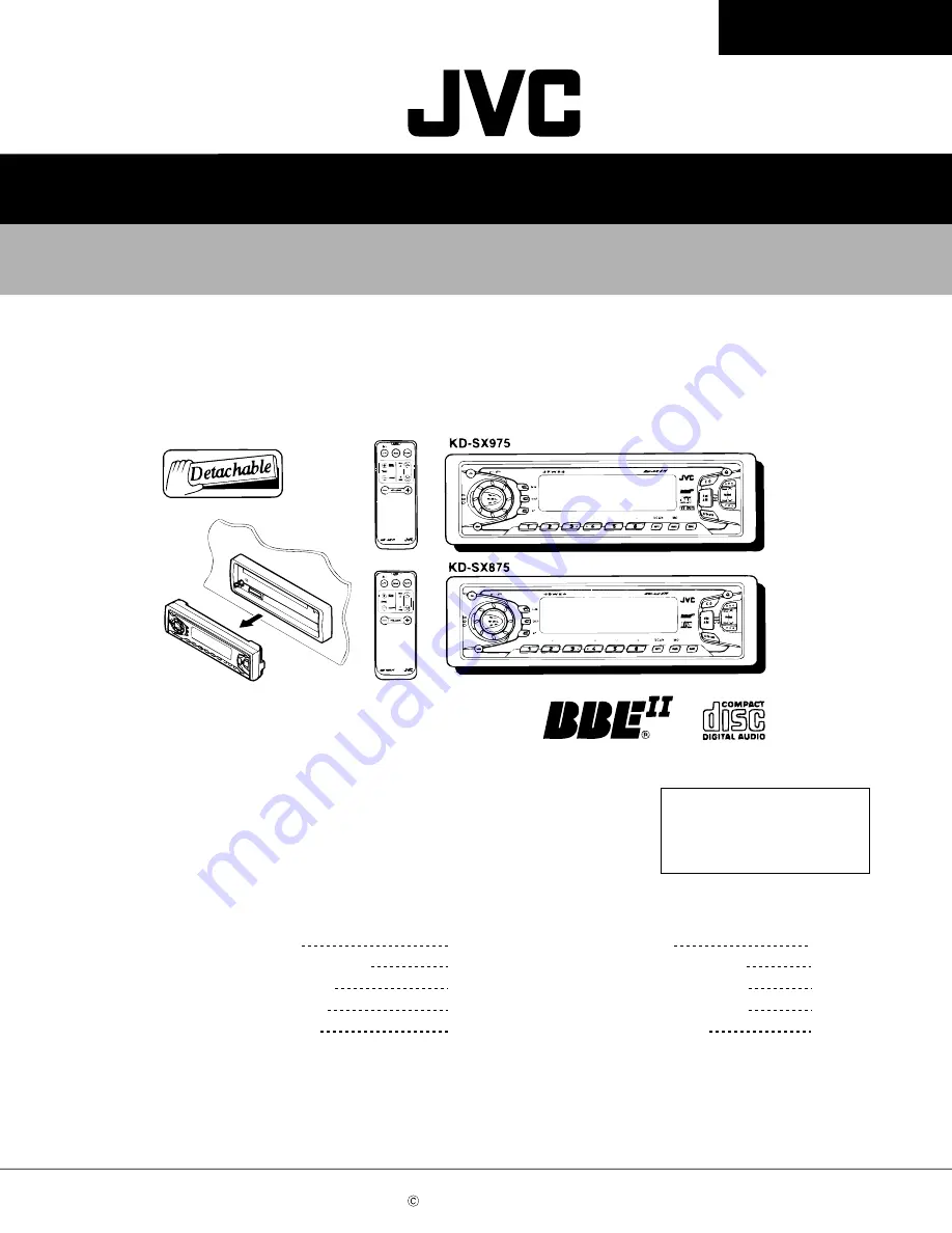
CD RECEIVER

No.49620

Feb. 2001

COPYRIGHT      2001 VICTOR COMPANY OF JAPAN, LTD.

KD-SX975 / KD-SX875

KD-SX975 / KD-SX875

Area Suffix

U ---- Other Areas

Contents

Safety precaution
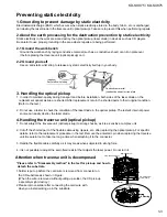
Preventing static electricity
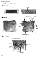
Location of main parts
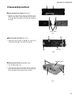
Disassembly method
Adjustment method

1-2
1-3
1-4
1-5
1-10

Flow of functional 
      operation unit TOC read
Maintenance of laser pickup
Replacement of laser pickup
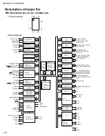
Discription of major ICs 

1-11

1-13
1-13
1-14

Содержание KD-SX875

Страница 1: ...KD SX875 Area Suffix U Other Areas Contents Safety precaution Preventing static electricity Location of main parts Disassembly method Adjustment method 1 2 1 3 1 4 1 5 1 10 Flow of functional operation unit TOC read Maintenance of laser pickup Replacement of laser pickup Discription of major ICs 1 11 1 13 1 13 1 14 ...

Страница 2: ...be left over on some parts of the chassis Therefore pay attention to such burrs in the case of preforming repair of this system Safety precaution Please use enough caution not to see the beam directly or touch it in case of an adjustment or operation check ...

Страница 3: ...eplacement return the shorted parts to their original condition Refer to the text 2 Do not use a tester to check the condition of the laser diode in the optical pickup The tester s internal power source can easily destroy the laser diode 4 Handling the traverse unit optical pickup 1 Do not subject the traverse unit optical pickup to strong shocks as it is a sensitive complex unit 2 Cut off the sho...

Страница 4: ...D mechanism Main board 16 pin connector Power IC Main board assembly Loading motor Damper Damper Damper Spindle motor Feed motor Optical pick up unit Mechanism relay board RCA jack Connector to front PCB Antenna jack Changer control connector Front PCB Display Tuner pack ...

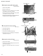
Страница 5: ...side Removing the heat sink See Fig 2 1 Remove the three screws B attaching the heat sink on the left side of the body and remove the heat sink Removing the bottom cover See Fig 3 1 2 Turn the body upside down Insert a screwdriver to the two joints c and two joints d on both sides of the body and the joint e on the back of the body then detach the bottom cover from the body Fig 1 Fig 2 Front chass...

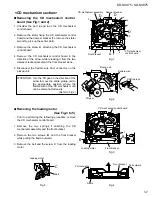
Страница 6: ...CD mechanism assembly Removing the CD mechanism assembly See Fig 6 1 2 3 4 Remove the front chassis Remove the bottom cover Remove the main amplifier board assembly Remove the three screws E attaching the CD mechanism assembly from the top cover Removing the control switch board See Fig 7 and 8 1 2 3 Remove the front chassis Remove the four screws F attaching the rear cover on the back of the fron...

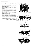
Страница 7: ...ire pickup unit to the appropriate position where the flexible wire of the CD mechanism unit can be disconnected easily Refer to Fig 2 ATTENTION Prior to performing the following procedure remove the CD mechanism control board Remove the two springs f attaching the CD mechanism assembly and the front bracket Remove the two screws B and the front bracket while pulling the flame outward Remove the b...

Страница 8: ... the two screws E and both sides rear damper brackets from the dampers Detach the CD mechanism assembly from the left side to the right side 1 2 3 4 Removing the CD mechanism assembly See Fig 1 6 to 9 The CD mechanism assembly can be removed if only the rear damper bracket on the left side is removed ATTENTION Fig 6 Fig 7 Fig 8 Fig 9 Rear damper bracket Fix arm R Damper D D Damper bracket CD mecha...

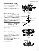
Страница 9: ... pickup mount nut from the pickup unit Pull out the FD screw 2 Removing the pickup unit See Fig 10 and 11 When reattaching the pickup unit reattach the part j of the pickup unit then the part i of the FD screw ATTENTION Prior to performing the following procedure remove the CD mechanism control board the front bracket loading motor the CD mechanism assembly and the feed motor assembly Turn up the ...

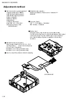
Страница 10: ...mpedance 4 4 to 8 allowance How to connect the extension cable for adjusting Standard volume position Balance and Bass Treble volume Indication 0 FM MW Dummy load Exclusive dummy load should be used for AM and FM For FM dummy load there is a loss of 6dB between SSG output and antenna input The loss of 6dB need not be considered since direct reading of figures are applied in this working standard E...

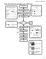
Страница 11: ...d RF signal eye pattern opens TOC readout Jump to the first track Play When the laser diode correctly emits Microprocessor commands SEL TC9462 LD CN501 No disc display When the disc correctly rotates Microprocessor commands DMO TC9462 Spindle motor IC581 5 Tracking Servo Loop ON RF signal Rough Servo Mode CLV Servo Mode Program Area CLV Servo Mode Lead In Area Digital 0 Flow of functional operatio...

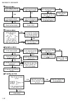
Страница 12: ... is moving 4V Does the S search waveform appear at IC581 pins 8 and 9 Check the circuits in the vicinity of IC501 pins 8 9 and 15 Check the pickup and its connections Is the disk rotated Does the RF signal appear at TP1 Is the RF waveform at TP1 distorted Proceed to the Tracking section Is 4V present at IC581 pins 4 and 5 Check the spindle motor and its wiring Check the circuits in the vicinity of...

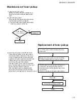
Страница 13: ...stics of the whole optical block do not touch the semi fixed resistor If the laser power is lower than the specified value the laser diode is almost worn out and the laser pickup should be replaced If the semi fixed resistor is adjusted while the pickup is functioning normally the laser pickup may be damaged due to excessive current Is RF output 1 3 0 4Vp p YES NO O K Replace it Replacement of las...

Страница 14: ...RFACE 3 UART0 8 INTERRUPT CONTROL BUZER OUTPUT SYSTEM CONTROL VOLTAGE REGULATOR PLL VOLTAGE REGULATOR PLL FREQUENCY COUNTER A D CONVERTER PORT 13 PORT 12 PORT10 PORT 7 PORT 6 PORT 5 PORT 4 PORT 3 PD178078 3Kbyte PD178076 2Kbyte RAM PD178078 60Kbyte PD178076 48Kbyte ROM 78k 0 CPU CPRE 16 bit TIMER EVENT COUNTER PORT 0 PORT 1 PORT 2 8 8 8 8 8 8 8 8 8 8 3 5 NC JBUS INT SW1 REMOCON PS1 PS2 DETACH NC K...

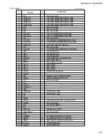
Страница 15: ...MUNICATION LINE JVC BUS COMMUNICATION LINE JVC BUS COMMUNICATION LINE JVC BUS COMMUNICATION LINE Non connection Non connection Non connection VOL IC COMMUNICATION LINE VOL IC COMMUNICATION LINE Non connection CD DRIVER COMMUNICATION LINE LCD DRIVER COMMUNICATION LINE JVC BUS OUTPUT SELECT Non connection LCD DRIVER COMMUNICATION LINE CD MECHA SW CD MECHA SW CD MECHA SW TRAVERSE MECHA REST SW ENCODE...

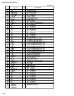
Страница 16: ...ection Non connection POWER CONT CD POWER CONT MUTE CONT Non connection BEEP FOR SW OPERATION Non connection Non connection Non connection Non connection Non connection Non connection Non connection Non connection Non connection CD MECHA DRIVER CONT CD MECHA DRIVER CONT CD LSI COMMUNICATION LINE CD LSI COMMUNICATION LINE CD LSI COMMUNICATION LINE CD LSI COMMUNICATION LINE CD LSI COMMUNICATION LINE...

Страница 17: ...975 KD SX875 1 17 REFR REFL FILTER 8 9 10 11 12 13 14 1 2 3 4 5 6 7 INR NFR FIL NFL CL Vcc INL CL LGND OUTL OUTR RGND CR CR 1 7 8 3220 14 BA3220FV X IC341 IC441 Line Out Amp 1 Terminal layout 2 Block diagram ...

Страница 18: ...nt Output Pin CH1 Rear Output Pin CH1 Front Output Pin CH1 Bass Filter Setting Pin CH1 Bass Filter Setting Pin CH2 Bass Filter Setting Pin CH2 Bass Filter Setting Pin CH2 treble Filter Setting Pin CH1 treble Filter Setting Pin CH2 treble Input Pin CH2 BBE II Signal Output Pin CH2 Output MIX Amplifier Inverse Input Pin A2 B2 C2 D2 FIL GND SI SC VCC OUTR2 OUTF2 OUTR1 OUTF1 BOUT1 BNF1 BOUT2 BNF2 TNF2...

Страница 19: ...MPOUT ANT CTRL VCC BATT DET AUDIO OUT CTRL CD OUT ILM AJ ILM OUT GND Output voltage is VCC 1 V when M or H level applied to CTRL pin Output voltage is VCC 1 V when M or H level to CTRL pin and H level to ANT CTRL Connected to ACC Regular 5 7V Output voltage is 5V when M or H level applies to CTRL pin Output for ACC detector L ANT output OFF H ANT output ON Connected to VCC Low battery detect Outpu...

Страница 20: ...tput Sample as Load Circuit 1 Sample as Load Circuit 1 Sample as Load Circuit 1 1k 1k S1 CL Input Output C L H H A X L H Y Z H L 1 2 3 4 5 6 7 14 13 12 11 10 9 8 HD74HC126FP X IC771 Buffer 1 Terminal layout 2 Block diagram 3 Pin function 1C 1A 1Y 2C 2A 2Y GND 3Y 3A 3C 4Y 4A 4C Vcc Note H High L Low X H and L Z H L X ...

Страница 21: ...external resistor and capacitor to this pin Serial data transfer inputs Connected to the controller CE Chip enable CL Synchronization clock DI Transfer data Display off control input INH L VSS Display forced off Used for applying the LCD drive 2 3 bias voltage externally Must be connected to VDD2 when a 1 2 bias drive scheme is used Used for applying the LCD drive 1 3 bias voltage externally Must ...

Страница 22: ... 2 OUT 2 PWR GND2 R F IN 3 IN 4 PRE GND ON TIME C Muting ON Time Control Circuit Protective circuit Protective circuit Mute circuit Ripple Filter Stand by Switch N C 0 22 F 2200 F 0 022 F 0 22 F TAB 5V ST ON 47 F 0 22 F 0 22 F 22 F Mute 10K 3 3 F OUT 3 OUT 3 Low Level Mute ON PWR GND3 OUT 4 OUT 4 PWR GND4 LA4743K IC351 Power AMP 1 Block diagram ...

Страница 23: ...19 20 21 22 23 24 25 Symbol Pin No Function Header of IC Power GND Outpur for front Rch Stand by input Output for front Rch Power input Output for rear Rch Power GND Output for rear Rch Ripple filter Rear Rch input Front Rch input Signal GND Front Lch input Rear Lch input Power on time control Output for rear Lch Power GND Output for rear Lch Power input Output for front Muting control input Outpu...

Страница 24: ...R 28 27 26 25 24 23 22 21 20 19 18 17 16 15 FR 1 2 3 4 5 6 7 8 9 10 11 12 13 14 FR CH 3 4 5 Power supply Output control CH5 CH4 CH2 CH1 CH3 22K 11K 5VREG PNPTr The outside putting 22K 22K 22K 11K 11K 11K CH1 2 Power supply LA6567H X IC581 CD DRIVER 1 Pin layout blockdiagram Level shift Level shift Level shift Level shift Thermal shutdown Input Signal system power supply ...

Страница 25: ... adjustment Regulator terminal Outside putting PNP base Regulator terminal Outside putting PNP collector Standard voltage input terminal Signal system power supply It is short with VCC1 VCC2 CH4 Input terminal For gain adjustment CH4 Input terminal 5CH VLO Output voltage set terminal Signal system GND 5CH VLO Signal output switch terminal FWD Input of logic of loading part 5CH VLO Signal output sw...

Страница 26: ...20k ohm 20k ohm 20k ohm 13k ohm 680 ohm 2 12k ohm BOTTOM PEAK 20k ohm 20k ohm 20k ohm 12k ohm 1 74k ohm 47k ohm 12k ohm 180k ohm 50uA 21k ohm 21k ohm 7 96k ohm 10k ohm 10k ohm 10k ohm 10k ohm 10pF 36pF 50k ohm 15k ohm 30k ohm 7 67k ohm 10k ohm 30k ohm 15k ohm 20uA 21k ohm 29k ohm 24k ohm 24k ohm 65uA 20pF 180k ohm 20pF 180k ohm 180k ohm 40pF 40pF I I I I SW3 SW2 SW1 1k ohm LOC 3 STATE DET 20pF TEO...

Страница 27: ...output polarity can invert by command Channel clock output terminal 44 1khz L ch at L level and R ch at H level the output polarity can invert by command REMARKS With pull up resistor UHSO H H L L HSO H L H L PLAYBACK SPEED Nomal 2 times 4 times Digital GND terminal Bit clock output terminal 1 4112MHz Audio data output terminal Digital data output terminal Buffer memory over signal output terminal...

Страница 28: ...utput 2VREF AVSS 3 state PWM signal output 2VREF VREF VSS PWM carrier 88 2kHz 3 state output 2VREF VREF VSS With pull up resistor With pull up resistor With pull up resistor 40 41 42 43 44 45 46 47 48 49 50 51 52 53 54 55 56 57 58 61 62 63 64 67 68 69 70 RFCT RFZI RFRP FEI SBAD TSIN TEI TEZI FOO TRO VREF RFGC TEBC FMO FVO DMO 2VREF SEL FLGA D VDD VSS IO0 3 DMOUT CKSE DACT RFRP signal center level ...

Страница 29: ...al for system clock Analog GND terminal for DA converter Rch R channel data forward output terminal Analog supply voltage terminal for DA converter Reference voltage terminal for DA converter L channel data forward output terminal Analog GND terminal for DA converter Lch Test mode terminal Normal keep at open Micon interface data input output terminal Digital power supply voltage terminal Digital ...

Страница 30: ...3 2 1 V B OUTPUT B INPUT B INPUT A INPUT A INPUT A OUTPUT V NJM4565M WE IC111 Ope amp RPM6938 SV4 IC602 Remote Censor Vcc Vcc Comp AGC AMP PD Detector BPF fo trimming circuit I V conversion magnetic shield Rout GND 22k 1 Block diagram ...

Страница 31: ...Printed in Japan 200102 V VICTOR COMPANY OF JAPAN LIMITED MOBILE ELECTRONICS DIVISION PERSONAL MOBILE NETWORK BUSINESS UNIT 10 1 1Chome Ohwatari machi Maebashi city Japan No 49620 KD SX975 KD SX875 ...

Страница 32: ...AR L R TUL R AM FM CH L R FM AM TUNER TU1 POWER AMP IC351 LA4743K LINE OUT J931 J1 E VOL IC301 BA3860K CHANGER CONTROL IC771 HD74HC126FP CD L R CD LPF IC111 NJM4565M VOL CL VOL DA IC341 441 L R CH LINE AMP BA3220FV SYSTEM CONTROLLER IC701 uPD178078GF 543 CN701 CN601 ENC 1 2 VOLUME JOG EN601 REMOCON KEY0 2 S1 S68 COM1 3 LCDDI LCDCLK LCDCE REMOTO CONTROL RECEIVER IC680 RPM6938 SV4 OPERATION SW S601 ...

Страница 33: ... M E M O KD SX975 KD SX875 2 2 ...

Страница 34: ...220FV 4 7uH 2SD601 LA4743K UN2211 2 2 50 0 001 BA3220FV 47 16 4 7 25 2 2 50 100 10 2 2 50 2 2 50 CRS03 1K 1SS355 X QSW0451 001 2 2 50 2 2 50 10K 330 1 5K 24K 24K 150K 33K 47 16 2200 16 2 2 50 2 2 50 100 10 100 10 100 10 100 22K 100k 10k 100 4 7 25 10 16 1M 1 50 47K 1SS133 47K 10K 4 7 25 2 2 50 10K QLD0033 001 2 2 50 2 2 50 4 7 25 24K 24K 150K 0 047 1K 10K 33K 33K 0 047 UN2211 12k 1SS133 10K 10 16 ...

Страница 35: ...0 01 2700P 0 01 0 033 10K 100 6 3 1 5K 15K 3300P 560P 100 6 3 0 01 100 6 3 3 3K RF 0 047 0 047 100 6 3 0 047 4 7 25 0 01 100 6 3 100 6 3 10K 100 6 3 0 01 100 6 3 0 01 330 0 01 4 7 25 24K 2 4K 8 2K 5 6K 20K QAX0662 001Z 0 01 47K 47K 100K 47K 100K 47K 24K 12K 33K 33K 12K 120P 120P TA2109F X 20K 1 10W 1000P 27P 100 6 3 100 6 3 100 6 3 33K 2SB1322 0 01 0 01 47K 0 1 0 1 100 10 100 6 3 0 01 0 047 6 8K 3...

Страница 36: ... 1 8W 1SS355 X NSPW310BS BRS UDZS5 1B X 470 1 8W 0 01 4 7 6 3 1 8W 1 8W 47K 1K 1 8W UN2211 0 22 4 7 6 3 330K 1SS355 X 1 8W 1SS355 X 270 1 8W 0 22 1SS355 X 270 1 8W 470 1 8W 220P 390K SML 310LT MN X QNZ0006 001 430 1 8W 1SS355 X 270 1 8W 390 1 8W 560 1 8W NSPW310BS BRS NSPW310BS BRS 470 1 8W 470 1 8W 2SB815 7 X 100 1SS355 X 1SS355 X LCDCE LCDDA LCDCL DIMMER GND 10V ACC5V LCDDA COM3 LCDCL LCDCE COM2...

Страница 37: ...1 R303 R305 R331 R332 R341 R342 R343 R344 R345 R346 R347 R351 R352 R353 R354 R371 R372 R375 R376 R401 R403 R405 R431 R432 R441 R442 R443 R444 R445 R446 R447 R451 R452 R453 R454 R471 R472 R475 R476 R501 R502 R503 R504 R505 R506 R507 R508 R509 R511 R512 R531 R532 R533 R534 R537 R541 R542 R543 R544 R545 R547 R571 R581 R582 R583 R584 R710 R711 R712 R713 R764 R734 R735 R718 R720 R722 R706 R707 R709 R75...

Страница 38: ... S608 S609 S610 S611 S613 S614 S615 S616 S617 S618 S619 S620 B601 B602 B603 S1B C601 C602 C603 C604 C605 C606 CN601 B604 D641 D642 D643 D656 D657 IC601 IC602 Q641 Q642 R601 R602 R603 R608 R609 R611 R612 R613 R620 R621 R622 R623 R630 R625 R626 R627 R628 R629 R641 R642 R643 R644 R645 R646 R651 R652 R653 R654 R655 R656 R657 R658 R661 R662 R663 R669 R670 R671 R624 D651 D654 D659 D653 D658 D652 D655 15...

Страница 39: ... assemblies are not available as service parts Contents Exploded view of general assembly and parts list CD mechanism assembly and parts list Electrical parts list Packing materials and accessories parts list KD SX975 KD SX875 3 2 3 5 3 8 3 14 Area suffix U Other Areas ...

Страница 40: ...ock No M M M 1 6 6 6 1 2 48 49 34 33 37 35 40 36 43 44 42 45 46 47 39 41 73 52 52 51 50 11 38 56 58 57 55 59 60 54 61 4 5 15 12 29 21 26 19 9 9 13 14 32 16 18 30 25 28 27 22 24 23 20 31 17 M a i n b o a r d 63 72 64 65 62 7 7 3 66 8 8 8 70 67 68 71 F r o n t b o a r d 69 10 53 74 ...

Страница 41: ...S3794 003 LOCK LEVER L 1 22 VKS3795 002 LOCK LEVER R 1 23 VKS5563 001 GEAR 1 24 VKZ4786 002 OIL DAMPER 1 25 FSKW4012 001 T SPRING 1 FOR L LEVER TOP 26 VKW5264 005 T SPRING 1 FOR RELEASE LEV 27 VKW5262 001 T SPRING 1 FOR L LEVER R 28 QYSDSF2006M SCREW 1 DAMPER L LEVER R 29 VKW5263 002 T SPRING 1 FOR L LEVER L 30 VKZ4777 001 MINI SCREW 1 LOCK LEVER O L 31 FSKW4013 002 T SPRING 1 FOR OPEN LEVER 32 VY...

Страница 42: ...4 001A LCD CASE 1 57 FSJK3028 001 LCD LENS 1 58 FSYH4061 001 LIGHTNG SHEET 2 59 FSYH4036 052 SHEET 1 60 FSKS3013 001 LENS CASE 1 61 GE30155 002A NAME PLATE 1 KD SX975 GE30154 002A NAME PLATE 1 KD SX875 62 VMA4652 001SS EARTH PLATE 1 63 FSKL4024 001 IC BRACKET 1 64 GE40103 001A REG BRACKET 1 65 GE40104 002B HEAT SINK 1 66 FSKM3010 017 REAR BRACKET 1 67 QYSDST2606Z SCREW 1 REAR BKT REG BK 68 QYSDST2...

Страница 43: ...0 71 5 7 91 4 3 7 6 19 18 105 48 43 50 41 42 103 49 49 d 56 107 131 36 107 107 d 38 32 33 130 106 29 108 106 135 104 107 40 63 39 a 51 52 109 132 86 113 113 134 80 117 92 84 c 79 88 93 22 22 89 62 81 82 116 102 101 108 100 133 57 Grease G 31SA G 31SA Bottom side RX 405 CD mechanism assembly and parts list Block No M M M 2 TN CCD1001Z 136J ...

Страница 44: ... 20 30310149T REAR DAM BKT Z 1 22 30310151T HUNG UP SP FZ 2 23 30310129T HUNG UP SP R 2 29 30300510T PU GEAR B 1 32 30310544T F M BASE Z 1 33 30310547T FD GR BLK Z 1 36 30310546T PU GUIDE Z 1 38 30310533T THRUST SPR M 1 39 30310548T PU M NUT Z 1 40 30310512T NUT PUSH SPR PL 1 41 30310558T CLP ARM Z 1 42 30310514T CLP ARM SPRING 1 43 30310552T CLAMPER Z 1 48 30310557T CLAMPER PLATE Z 1 49 30310524T...

Страница 45: ...J 1 100 9C0620503T C B TAP SCREW 2 M2X5 101 9C2020401T C SCREW TS G 5 M2X4 102 9C4320403T C B TAP SCREW 4 M2X4 103 9C0117223T SCREW 2 M1 7X2 2 104 9C0917703T C TAP SCREW S3 1 M1 7X7 105 9C0320201T C TAP SCREW S3 1 M2X2 106 9C4920013T C TAP SCREW S3 2 M2X10 107 9C4920603T C TAP SCREW B3 4 M2X6 108 9P0220031T TAMS SCREW 2 M2X3 109 9C0314203T C TAP SCREW 1 M1 4X2 110 9C0420253 C TAP SCREW 1 M2X2 5 11...

Страница 46: ...52 QERF1HM 225Z E CAPACITOR 2 2MF 20 50V C 353 NCS31HJ 391X C CAPACITOR C 354 NCS31HJ 391X C CAPACITOR C 355 QERF1CM 107Z E CAPACITOR 100MF 20 16V C 356 NCB31HK 223X C CAPACITOR C 357 NCB31HK 223X C CAPACITOR C 358 QER41CM 476 E CAPACITOR 47MF 20 16V C 359 QERF1CM 226Z E CAPACITOR 22MF 20 16V C 361 QEK41EM 475 E CAPACITOR 4 7MF 20 25V C 362 QEK41EM 475 E CAPACITOR 4 7MF 20 25V C 372 NCS31HJ 271X C...

Страница 47: ...C 968 QER41AM 227 E CAPACITOR 220MF 20 10V C 969 QER41AM 227 E CAPACITOR 220MF 20 10V C 970 NCB31EK 104X C CAPACITOR C 971 QERF1CM 226Z E CAPACITOR KD SX975 C 975 NCB31EK 103X C CAPACITOR C 976 QERF0JM 476Z E CAPACITOR 47MF 20 6 3V C 977 QERF1CM 107Z E CAPACITOR 100MF 20 16V C 981 NCB31EK 104X C CAPACITOR C 982 NCB31EK 104X C CAPACITOR C 983 NCB31EK 104X C CAPACITOR C 984 NCB31EK 104X C CAPACITOR ...

Страница 48: ...TOR R 305 NRSA63J 332X MG RESISTOR R 321 NRSA63J 222X MG RESISTOR R 322 NRSA63J 222X MG RESISTOR R 323 NRSA63J 0R0X MG RESISTOR KD SX875 R 324 NRSA63J 0R0X MG RESISTOR KD SX875 R 331 NRSA63J 103X MG RESISTOR KD SX975 R 332 NRSA63J 103X MG RESISTOR KD SX975 R 341 NRSA63J 333X MG RESISTOR KD SX975 R 342 NRSA63J 273X MG RESISTOR KD SX975 R 343 NRSA63J 333X MG RESISTOR KD SX975 R 344 NRSA63J 273X MG R...

Страница 49: ...31 NRSA63J 473X MG RESISTOR R 732 NRSA63J 103X MG RESISTOR R 733 NRSA63J 473X MG RESISTOR R 734 NRSA63J 104X MG RESISTOR R 735 NRSA63J 103X MG RESISTOR R 737 NRS181J 511X MG RESISTOR R 744 NRSA63J 222X MG RESISTOR R 745 NRSA63J 222X MG RESISTOR R 746 NRSA63J 103X MG RESISTOR R 747 NRSA63J 472X MG RESISTOR R 749 NRSA63J 0R0X MG RESISTOR KD SX975 R 750 NRSA63J 122X MG RESISTOR R 751 NRSA63J 103X MG ...

Страница 50: ... 122X MG RESISTOR R 609 NRSA63J 182X MG RESISTOR R 611 NRSA63J 272X MG RESISTOR R 612 NRSA63J 821X MG RESISTOR R 613 NRSA63J 821X MG RESISTOR R 614 NRSA63J 122X MG RESISTOR R 615 NRSA63J 182X MG RESISTOR R 616 NRSA63J 272X MG RESISTOR R 617 NRSA63J 392X MG RESISTOR R 620 NRS181J 471X MG RESISTOR R 621 NRS181J 271X MG RESISTOR KD SX875 R 621 NRS181J 681X MG RESISTOR KD SX975 R 622 NRS181J 271X MG R...

Страница 51: ...3 13 KD SX975 KD SX875 M E M O ...

Страница 52: ...3 14 KD SX975 KD SX875 Packing materials and accessories parts list Block No M M M 3 Block No M M M 4 P7 P2 P4 P1 P5 P7 P3 A1 A3 A12 A14 A9 A10 A11 KIT A4 A8 A13 P6 ...

Страница 53: ...sories Q ty Description Block No M4MM A 1 GET0020 001A INST BOOK 1 A 2 GET0020 002A INSTALL MANUAL 1 A 3 GET0020 003A INSTALL MANUAL 1 THA A 4 VKZ4027 202 PLUG NUT 1 A 5 VKH4871 001SS MOUNT BOLT 1 A 6 VKZ4328 001 LOCK NUT 1 A 7 WNS5000Z WASHER 1 A 8 FSKL4010 002 HOOK 2 A 9 RM RK31 REMOCON 1 A 10 QAB0014 001 BATTERY 1 A 11 FSJB3001 30C HARD CASE 1 A 12 FSKM2004 202 MOUNTING SLEEVE 1 A 13 FSJD2034 0...

Отзывы: