background image

KD-SC800R

1-16 (No.49820)

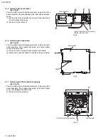
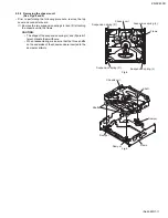
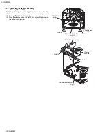
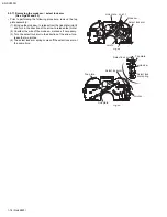
2.2.11 Removing the mode sw. / select lock arm 

(See Figs.22 and 23)

• Prior to performing the following procedure, remove the top

plate assembly.

(1) Bring up the mode sw. to release from the link plate (joint 

t

)

and turn in the direction of the arrow to release the joint 

u

.

(2) Unsolder the wire of the mode sw. marked s if necessary.
(3) Turn the select lock arm in the direction of the arrow to re-

lease the two joints 

v

.

(4) The select lock arm spring comes off the select lock arm at

the same time.

Fig.22

Fig.23

Mode sw.

Select lock arm

Joint t

Link plate

Joint u

s

Top plate

Top plate

Select lock arm

Select lock 
arm spring

Select lock arm

Link plate

Joints v

Hook w

Содержание KD-SC800R

Страница 1: ... 49820 2003 04 KD SC800R CD RECEIVER 49820 2003 04 KD SC800R TABLE OF CONTENTS 1 Important Safety Precautions 1 2 2 Disassembly method 1 4 3 Adjustment 1 24 4 Description of major ICs 1 28 COMPACT DIGITAL AUDIO Area Suffix E Continental Europe EX Central Europe ...

Страница 2: ...autions Burrs formed during molding may be left over on some parts of the chassis Therefore pay attention to such burrs in the case of preforming repair of this system Please use enough caution not to see the beam directly or touch it in case of an adjustment or operation check ...

Страница 3: ...iode in the optical pickup The tester s internal power source can easily destroy the laser diode 1 3 Handling the traverse unit optical pickup 1 Do not subject the traverse unit optical pickup to strong shocks as it is a sensitive complex unit 2 Cut off the shorted part of the flexible cable using nippers etc after replacing the optical pickup For specific details refer to the replacement procedur...

Страница 4: ...e front panel assembly 1 Remove the screw A on the both sides of the main body 2 Remove the two screws B on the front side of the main body 3 Release the two joints a and two joints b on both sides of the main body using a screwdriver and remove the front chassis assembly forward 4 Release the two joints c on the bottom side of the main body and remove the front chassis assembly in the direc tion ...

Страница 5: ... 7 Prior to performing the following procedure remove the front panel assembly front chassis assembly and heat sink 1 Turn over the body and release the two joints d two joints e and joint f CAUTION Do not damage the main board when releasing the joint d us ing a screwdriver See Figs 6 and 7 Fig 6 Fig 7 C D Heat sink Joint d Joint e Joint f Bottom cover Joint e Joint d Joint f Bottom cover ...

Страница 6: ...cedure remove the front panel assembly front chassis assembly heat sink bottom cover and rear bracket 1 Remove the two screws H attaching the main board 2 Disconnect connector CN501 and remove the main board Fig 9 2 1 7 Removing the CD mechanism assembly See Fig 10 Prior to performing the following procedure remove the front panel assembly front chassis assembly heat sink bottom cover rear bracket...

Страница 7: ... Prior to performing the following procedure remove the front panel assembly 1 Remove the four screws K on the back side of the front panel assembly 2 Release the ten joints g 3 Take out the front board Fig 11 Fig 12 Fig 13 K K K Joint g Joint g Joint g Joint g Front board ...

Страница 8: ...2 1 Removing the top cover See Figs 1 and 2 1 Remove the two screws A on the both side of the body 2 Lift the front side of the top cover and move the top cover backward to release the two joints a Fig 1 Fig 2 A A A Joints a Top cover Joints a Top cover ...

Страница 9: ...nnector board 2 Solder the short circuit point on the connector board 3 Disconnect the flexible wire from the pickup 4 Move the connector board in the direction of the arrow to release the two joints b 5 Unsolder the wire on the connector board if necessary CAUTION Unsolder the short circuit point after reassembling Fig 3 Fig 4 Fig 5 B Connector board Pickup Short circuit point Joints b Wires Pick...

Страница 10: ...e DET switch See Figs 6 and 7 1 Extend the two tabs c of the feed sw holder and pull out the switch 2 Unsolder the DET switch wire if necessary Fig 6 Fig 7 Connector board DET switch Pickup DET switch Tab c Tab c DET switch wire Feed sw holder ...

Страница 11: ...ing the chassis unit to the frame CAUTION The shape of the suspension spring L and R are dif ferent Handle them with care When reassembling make sure that the three shafts on the underside of the chassis unit are inserted to the dampers certainly Fig 8 Fig 9 Suspension spring L Suspension spring L Suspension spring R Suspension spring R Chassis unit Frame Chassis unit Frame Shafts Shaft Damper Dam...

Страница 12: ... procedure remove the top cover 1 Remove the clamper arm spring 2 Move the clamper assembly in the direction of the arrow to release the two joints d Fig 10 Fig 11 Clamper arm spring Chassis rivet assembly Joint d Joint d Clamper assembly Clamper arm spring Clamper assembly Joint d Joint d Chassis rivet assembly ...

Страница 13: ... Remove the screw C and move the loading feed motor assembly in the direction of the arrow to remove it from the chassis rivet assembly 2 Disconnect the wire from the loading feed motor assembly if necessary CAUTION When reassembling connect the wire from the loading feed motor assembly to the flame as shown in Fig 12 Fig 12 Fig 13 Loading feed motor assembly Loading feed motor assembly C ...

Страница 14: ...screw F 2 Reattach the feed sw holder to the feed rack while setting the joint g to the slot of the feed rack and setting the part f of the feed rack to the switch of the feed sw holder correct ly 3 As the feed sw holder is temporarily attached to the pickup unit set to the gear of the joint g and to the bending part of the chassis joint h at a time CAUTION Make sure that the part i on the undersi...

Страница 15: ...at the slot of the chassis rivet assembly respectively and join the joint k at a time Fig 19 Fig 20 2 2 10 Removing the top plate assembly See Fig 21 Prior to performing the following procedure remove the top cover connector board chassis unit and clamper assembly 1 Remove the screw H 2 Move the top plate assembly in the direction of the arrow to release the two joints r 3 Unsolder the wire marked...

Страница 16: ...the direction of the arrow to release the joint u 2 Unsolder the wire of the mode sw marked s if necessary 3 Turn the select lock arm in the direction of the arrow to re lease the two joints v 4 The select lock arm spring comes off the select lock arm at the same time Fig 22 Fig 23 Mode sw Select lock arm Joint t Link plate Joint u s Top plate Top plate Select lock arm Select lock arm spring Selec...

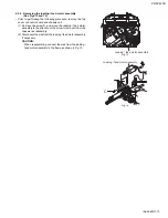
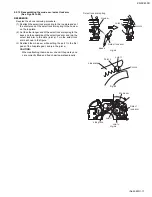
Страница 17: ... x on the underside of the select lock arm and join the select lock arm to the slots joint v Turn the select lock arm as shown in the figure 3 Reattach the mode sw while setting the part t to the first peak of the link plate gear and join the joint u CAUTION When reattaching the mode sw check if the points y and z are correctly fitted and if each part operates properly Fig 24 Fig 25 Fig 26 Select ...

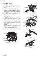
Страница 18: ...Figs 29 and 30 REFERENCE Reverse the above removing procedure 1 Reattach the link plate spring 2 Reattach the link plate to the link plate spring while joining them at joint d 3 Reattach the joint a of the select arm R to the first peak of the link plate while joining the two joints b with the slots Then turn the select arm R as shown in the figure The top plate is joined to the joint c CAUTION Wh...

Страница 19: ...plate 5 Extend the lock arm rivet assembly outward and release the joint j from the boss of the chassis rivet assembly The roller guide springs on both sides come off at the same time CAUTION When reassembling reattach the left and right roller guide springs to the lock arm rivet assembly before reat taching the lock arm rivet assembly to the chassis rivet assembly Make sure to fit the part k of t...

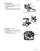
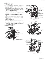
Страница 20: ...over chassis unit pickup unit and top plate assembly 1 Remove the screw K attaching the loading gear bracket The loading gear 6 and 7 come off the loading gear brack et 2 Pull out the loading gear 5 Fig 35 Fig 36 K Loading gear bracket Loading gear 6 Loading gear 5 Loading gear 3 K Loading gear bracket Loading gear 6 Loading gear 5 Loading gear 7 ...

Страница 21: ...off 7 Remove the loading gear 1 8 Move the change plate rivet assembly in the direction of the arrow to release from the three shafts of the chassis rivet assembly upward See Fig 38 9 Detach the loading gear plate rivet assembly from the shaft of the chassis rivet assembly upward while releasing the joint p See Figs 38 and 40 10 Pull out the loading gear 4 Fig 37 Fig 38 Fig 39 Fig 40 Slot m Slot m...

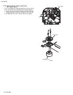
Страница 22: ...llowing procedure remove the top cover connector board chassis unit and clamper assembly 1 Remove the two screws L attaching the spindle motor as sembly through the slot of the turn table on top of the body 2 Unsolder the wire on the connector board if necessary Fig 41 Fig 42 L Turn table L Turn table Spindle motor ...

Страница 23: ...KD SC800R No 49820 1 23 2 3 Finder Plate Design Model Name KD SC800R Factory Setting Design Name SAPPHIRE BLUE Design Name LEOPARD Design Name SILVER HAIRLINE Design Name CARBON BLACK ...

Страница 24: ...hould be used for AM and FM For FM dummy load there is a loss of 6dB between SSG output and antenna input The loss of 6dB need not be considered since direct reading of figures are applied in this working standard Standard volume position Balance and Bass Treble volume lndication 0 Loudness OFF Frequency Band FM 87 5 MHz to 108 0 MHz AM MW 522 kHz to 1620 kHz LW 144 kHz to 279 kHz The cardboard is...

Страница 25: ...attern remains closed Tracking loop closed RF signal eye pattern opens TOC read out Jump to the first track Play When the laser diode correctly emits Microprocessor commands SEL TC94A14FA 38 LD CN501 15 No disc display When the disc correctly rotates Microprocessor commands DMO TC94A14FA 41 Spindle motor IC501 7 Tracking Servo Loop ON RF signal Rough Servo Mode CLV Servo Mode Program Area CLV Serv...

Страница 26: ...ar at IC501 pins 8 and 9 Check the circuits in the vicinity of IC501 pins 8 9 and 15 Check the pickup and its connections NO NO NO NO YES YES YES YES YES Is the disk rotated Does the RF signal appear at RF test point Is the RF waveform at RF test point distorted Proceed to the Tracking section Is 4V present at IC501 pins 6 and 7 Check the spindle motor and its wiring Check the circuits in the vici...

Страница 27: ...le optical block do not touch the semi fixed resistor If the laser power is lower than the specified value the laser diode is almost worn out and the laser pickup should be re placed If the semi fixed resistor is adjusted while the pickup is functioning normally the laser pickup may be damaged due to excessive current 3 4 Replacement of laser pickup Is RF output 1 0 0 35Vp p Replace it NO YES O K ...

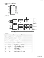
Страница 28: ... CTRL L ANT output OFF H ANT output ON 8 VCC Connected to VCC 9 BATT DET Low battery detect 10 AUDIO OUT Output voltage is 9V when M or H level applied to CTRL pin 11 CTRL L BIAS OFF M BIAS ON H CD ON 12 CD OUT Output voltage is 8V when H level applied to CTRL pin 13 ILM AJ Adjustment pin for ILM output voltage 14 ILM OUT Output voltage is 10V when M or H level applied to CTRL pin 15 GND Connected...

Страница 29: ... I Chip select 7 CCLK I Control data input terminal 8 CDTI I Control data input terminal 9 AOUTR O Rch negative analog output terminal 10 AOUTR O Rch positive analog output terminal 11 AOUTL O Lch negative analog output terminal 12 AOUTL O Lch positive analog output terminal 13 VSS Connect to ground 14 VDD Power supply terminal 15 DZFR O Rch data zero input detection terminal 16 DZFL O Lch data ze...

Страница 30: ...Y Vcc 1 2 Vcc 3 4 OUT 1 OUT 1 PWR GND1 OUT 2 OUT 2 PWR GND2 R F IN 3 IN 4 PRE GND ON TIME C Muting ON Time Control Circuit Protective circuit Protective circuit Mute circuit Ripple Filter Stand by Switch N C 0 22 F 2200 F 0 022 F 0 22 F TAB 5V ST ON 47 F 0 22 F 0 22 F 22 F Mute 10K 3 3 F OUT 3 OUT 3 Low Level Mute ON PWR GND3 OUT 4 OUT 4 PWR GND4 ...

Страница 31: ... 3 FR Outpur for front Rch 16 ONTIME Power on time control 4 STDBY Stand by input 17 RL Output for rear Lch 5 FR Output for front Rch 18 GND Power GND 6 VP1 Power input 19 RL Output for rear Lch 7 RR Output for rear Rch 20 VP3 Power input 8 GND Power GND 21 FL Output for front 9 RR Output for rear Rch 22 MUTE Muting control input 10 RIPPLE Ripple filter 23 FL Output for front 11 RRIN Rear Rch inpu...

Страница 32: ...ND VIN1 SW MUTE VREFIN VCCS 3 3VREG REGIN VIN2G VIN2 VIN3G VIN3 FR VIN1 A VIN1 A VCCP1 VO VO VO2 VO2 VO3 VO3 VO4 VO4 VCCP2 VIN4 VIN4G FR H L VIN1_SW H OP AMP_A L OP AMP_B 33k 11k Signal system power supply All outputs ON OFF H ON L OFF MUTE Level shift Level shift Power system GND Signal system power supply 3 3VREG External PTP Tr Power system GND Level shift Level shift 33k 11k 11k 33k 33k 11k ...

Страница 33: ...supply 13 VIN4 Input pin for channel 4 14 VIN4G Input pin for channel 4 for gain adjustment 15 VIN3 Input pin for channel 3 16 VIN3G Input pin for channel 3 for gain adjustment 17 VIN2 Input pin for channel 2 18 VIN2G Input pin for channel 2 for gain adjustment 19 REGIN External PNP transistor base connection 20 3 3VREG 3 3VREG output pin external PNP transistor collector connection 21 VCCS Signal...

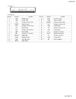
Страница 34: ...ge externally Must be connected to VDD1 when a 1 2 bias drive scheme is used 60 Vss Power supply connection Connect to GND 61 OSC I O Oscillator connection An oscillator circuit is formed by connecting an external resistor and capacitor at this pin 62 CE I Serial data interface connection to the controller CE Chip enable 63 CL I Serial data interface connection to the controller CL Sync clock 64 D...

Страница 35: ...P F 4 7 RPM6938 SV4 IC602 Remote control receiver Pin diagram Block diagram 8 7 6 5 4 3 2 1 V B OUTPUT B INPUT B INPUT A INPUT A INPUT A OUTPUT V 1 2 3 Vcc Vcc Comp AGC AMP PD Detector BPF fo trimming circuit I V conversion magnetic shield Rout GND 22k ...

Страница 36: ... comparator 8 SCOUT Sub carrier output of reconstruction filter 9 MODE Oscillator mode test control input 10 TEST Test enable input 11 GND Ground for digital part 0V 12 Vdd 5V supply voltage for digital part 13 OSCI Oscillator input 14 OSCO Oscillator output 15 T57 57 kHz clock signal output 16 CLK RDS clock output ANTI ALIASING FILTER CLOCKED COMPARATOR COSTAS LOOP VARIABLE AND FIXED DIVIDER 57 k...

Страница 37: ...left front 5 TL I Treble control capacitor left channel or input from an external equalizer 6 B2L Bass control capacitor left channel or output to an external equalizer 7 B1L Bass control capacitor left channel 8 IVL I Input volume 1 left control part 9 ILL I Input loudness left control part 10 QSL O Output source selector left channel 11 IDL Not used 12 MUTE Not used 13 ICL I Input C left source ...

Страница 38: ...k 20k 3k 180k 240k 240k 15pF 15pF 40pF 40pF 10pF 60k 60k 22k 22k 94k 94k 14k 50k 20k 20k 20k 40k 50k PEAK 15k 40k 2k 1 75k 1 3V 2k 1k 180k 3k 12k 12k 20k 40k 30k 10pF 50 A BOTTOM PEAK K 1 x0 5 x2 x0 5 x2 PIN SEL APC SW TEB TE BAL RFGC AGC Gian TEB TE BAL VCTRLPIN VCC APC ON 50 12dB Normal mode 0dB HiZ APC ON 0 6dB Normal mode 0dB GND APC OFF LDO H 50 0dB CD RW mode 12dB ...

Страница 39: ...cking search system 12 RFDC O RF signal peak detection output pin 13 GVSW I AGC FE TE amp gain change pin 14 VRO O Reference voltage VRO output pin VRO 1 2VCC When VCC 3 3V 15 FEO O Focus error signal generation amp output pin 16 FEN I Focus error signal generation amp negative phase input pin 17 RFRP O Signal amp output pin for track count Combining RFRP signal and TEO signal with TC94A14F FA con...

Страница 40: ...put pin L for L channel and H for R channel Output polarity can be inverted by command 3 AOUT O Audio data output pin MSB first or LSB first selectable by command 4 DOUT O Digital data output pin Outputs up to double speed playback 5 IPF O Correction flag output pin When set to H AOUT output cannot be corrected by C2 correction processing 6 VDD3 Digital 3 3V power supply voltage pin 7 VSS3 Digital...

Страница 41: ... H output with UHS H 39 AVDD3 Analog 3 3V power supply voltage pin 40 FMO O Feed equalizer output pin 41 DMO O Disc equalizer output pin 42 VSS3 Digital GND pin 43 VDD3 Digital 3 3V power supply voltage pin 44 TESIN I Test input pin Normally fixed to L 45 XVSS3 System clock oscillator GND pin 46 XI I System clock oscillator input pin 47 XO O System clock oscillator output pin 48 XVDD3 System clock...

Страница 42: ...7 46 45 44 43 42 41 40 39 38 37 DIT DAC DAC Bus Switch Address calc 2sets General output port C Pointer register Y Pointer register X Pointer register ERAM 2k word CROM 4k word 7 Y RAM 4k word X RAM 4k word Flag Timer register X0 X1 X2 Y0 Y1 Y2 MX AX AY MY MZ ALU A2 A1 A0 A3 round limit round limit Audio I F Microcom I F MAC Program control Instruction decoder PROM 4k 3 12k word PRAM 256word 1Mbit...

Страница 43: ...voltage for DAC Rch 28 VSSR GND for DAC R ch 29 TESTP I Test terminal H test mode L normal 30 TXO O SPDIF output 31 34 Po0 Po3 O General purpose output 0 3 35 VDDT Power supply for digital 3 3V 36 38 Po4 Po6 O General purpose output 4 6 39 REQ O REC terminal 40 VSS GND for digital 41 IRO I O External interrupt input 42 VDDM Internal 1Mbit SRAM power supply 2 5V 43 44 Fi0 Fi1 I Flug input 0 1 45 VS...

Страница 44: ...O NC 16 LCD CE O LCD DRIVER 17 SW2 I CD MECHA 18 PSW I CD MECHA 19 LED RED O LED 20 LED BLUE O LED 21 VOL 1 I ENCODER 22 VOL 2 I ENCODER 23 KEY0 I KEY 24 KEY1 I KEY 25 KEY2 I KEY 26 LEVEL I LEVEL DET 27 AVDD D VDD 28 SM I T PACK 29 SQ I SQ CIR 30 DOOR SW I DOOR SW 31 NO USE I P D 32 AVSS D GND 33 REGCPU E CAP 34 VDD D VDD 35 REGOSC E CAP 36 X2 X TAL 37 X1 I 38 GND0 D GND 39 SD ST I T PACK 40 GND2 ...

Страница 45: ...CE output for CD LSI 73 BUS0 I O data output and input 0 for CD LSI 74 BUS1 I O data output and input 1 for CD LSI 75 BUS2 I O data output and input 2 for CD LSI 76 BUS3 I O data output and input 3 for CD LSI 77 RST O CD LSI COMMUNICATION LINE 78 PS1 I ACC DETECTION INPUT 79 PS2 I MEMORY DETECTION 80 DETACH I DETACH DETECTION 81 RDS SCK I RDS clock input 82 GND1 83 MONO O MONO BY FORCE 84 SEEK STO...

Страница 46: ... No 49820 AV MULTIMEDIA COMPANY MOBILE ENTERTAINMENT CATEGORY 10 1 1chome Ohwatari machi Maebashi city 371 8543 Japan VICTOR COMPANY OF JAPAN LIMITED 200304WPC Printed in Japan KD SC800R ...

Страница 47: ...diagrams Printed circuit boards 2 1 2 2 2 5 to 7 CD ROM No SML200304 KD SC800R SCHEMATIC DIAGRAMS CD RECEIVER No 49820SCH 2003 04 COPYRIGHT 2003 VICTOR COMPANY OF JAPAN LTD KD SC800R KD SC800R Area Suffix E Continental Europe EX Central Europe ...

Страница 48: ...eft over on some parts of the chassis Therefore pay attention to such burrs in the case of preforming repair of this system Safety precaution Please use enough caution not to see the beam directly or touch it in case of an adjustment or operation check ...

Страница 49: ... KEY1 KEY2 ENC1 ENC2 REMOCON IC601 LCD DRIVER LCD1 CN701 TU1 FM AM TUNER IC701 MICOM IC161 E VOL IC71 RDS DETECTER FMEO AMEO FM AM IFC MONO S METER SD ST SK ST1 IC301 POWER AMP IC901 REGULATOR SPK BATTERY EACH BLOCK L CH R CH OUTLF OUTRF OUTLR OUTRR REAR L REAR R FRONT L FRONT R CD L CD R J301 LINE OUT LF LF RF RF LR LR RR RR COM1 COM2 COM3 S1 to S50 LCDCE LCDDA LCDCL SCL SDA RDSSCK RDSDA J1 ANT S...

Страница 50: ...10K 1K 1K 100p 47K 2 2 50 47K 10K 100 100K 100K 10K 100K 100 22K 100K 100K 0 047 0 1 2SD601A R X QAX0406 002Z 22p 33p 0 QAM0461 001 0 01 UN2111 X 15K 4 7K 4 7K 4 7K 470 0 12 1SS355 X 0 012 2 7K 1K 4 7 50 0 047 12K 1K 1 50 1 50 10K 10K 47K 47K 47K 1K 100p 2 2K 10K 0 1 47K 0 01 47K UN2211 X RB160M 30 X 47 16 0 082 QNZ0112 001 UN2211 X 220 10 100 10 0 1 1K 1SS355 X 47K 2SA1037AK RS X 12K 27K UN2211 X...

Страница 51: ... 2K 0 033 0 0 0 047 0 047 100 6 3 100 6 3 100 6 3 10k 0 01 1A3G T1 820 0 01 100 100 10 100 6 3 0 0068 0 18K 0 330K 82K 330K 82K 150 100 6 3 150 4 7K 47 6 3 8 2K 18K 6 8K 4 7 25 15K 0 4 7 25 1 5K 47 6 3 1M 100 16 33K 12K 33K 33K 12K 120p 120p 0 01 1 5K 1 5K 0 047 0 047 0 047 0 047 47u 47u 47u 47u 100p 100 6 3 100 10 1 50 22K 22K 2SB1322 RS T 0 001 0 01 56K 0 1 0 1 47p 0 047 100 100 0 047 100 100 0 ...

Страница 52: ... 2K 10K 10K 10K 1 2K 820 3 9K 820 820 2 7K 1 8K 1 2K 820 1 2K 1 8K 2 2K 820 QLD0253 001 NNZ0087 001 10K 680 820 510 10K 470 4 7 6 3 0 012 82 2SD601A R X 10 6 3 680 560 510 820 100 UDZS5 1B X 510 820 560 0 022 510 820 680 0 022 680 560 560 560 560 SML 310LT MN X UDZS6 2B X 10 51K 0 022 680p 680 680 UDZS6 2B X 2SD601A R X 0 01 820 UDZS6 2B X 680 0 01 2SD601A R X 82 680 680 10 680 UDZS6 2B X UDZS6 2B...

Страница 53: ... D321 D341 D561 R765 D891 D901 IC71 IC161 IC301 IC501 IC521 IC561 IC571 IC701 IC801 IC901 J1 J301 J801 L1 L521 L522 L523 L524 L701 L702 L901 Q2 Q3 Q51 Q52 Q53 Q71 Q72 Q73 Q74 Q321 Q341 Q501 Q561 Q782 Q783 Q891 Q901 Q902 R3 R4 R5 R9 R52 R53 R54 R55 R56 R57 R58 R72 R74 R75 R76 R162 R163 R173 R247 R323 R333 R343 R353 R503 R504 R505 R506 R507 R508 R509 R510 R515 R517 R523 R525 R526 R529 R530 R533 R534...

Страница 54: ...D702 D703 D704 D705 D706 D707 D708 D709 D781 D783 D892 D901 D902 D903 D904 IC301 IC901 J1 J301 J801 L1 L521 L522 L523 L524 L701 L702 L901 LM MSW Q1 Q4 Q5 Q6 Q7 Q31 Q32 Q41 Q42 Q241 Q331 Q351 Q501 Q521 Q522 Q561 Q781 R1 R2 R6 R7 R8 R10 R11 R31 R32 R33 R35 R41 R42 R43 R44 R45 R51 R59 R71 R73 R81 R82 R91 R92 R161 R164 R165 R166 R167 R168 R171 R172 R174 R175 R176 R177 R178 R184 R191 R194 R241 R242 R24...

Страница 55: ...R607 R608 R609 R610 R612 R613 R615 S601 S602 S603 S604 S605 S606 S607 S608 S609 S610 S611 S612 S614 S615 S616 S617 S618 C601 C602 C603 C611 C612 C681 C682 C692 C691 C694 C693 CN601 D641 D642 D643 D646 D692 D694 R689 IC602 EN601 Q691 Q692 Q693 Q694 R614 R631 R632 R633 R634 R635 R636 R637 R638 R639 R640 R641 R642 R643 R644 R645 R646 R647 R651 R652 R653 R657 R658 R661 R662 R671 R672 R673 R681 R693 R6...

Страница 56: ...KD SC800R VICTOR COMPANY OF JAPAN LIMITED AV MULTIMEDIA COMPANY 10 1 1Chome Ohwatari machi Maebashi city 371 8543 Japan No 49820SCH Printed in Japan 2003 04 ...

Страница 57: ...rvice parts Contents Exploded view of general assembly and parts list Block No M1 CD mechanism assembly and parts list Block No MB Electrical parts list Block No 01 02 Packing materials and accessories parts list Block No M3 M5 KD SC800R 3 2 3 4 3 6 3 12 Area suffix E Continental Europe EX Central Europe ...

Страница 58: ...rd Main board Front Front board board 14 A LCD1 LCD1 6 6 51 52 46 47 45 32 31 40 39 48 37 44 50 49 42 34 34 33 35 35 36 38 43 41 54 54 54 53 56 59 58 55 63 5 4 2 6 1 54 24 17 27 12 28 16 15 23 18 19 29 11 11 7 7 3 13 13 70 72 9 71 64 57 25 20 9 22 26 21 30 61 62 60 8 8 8 66 65 68 69 67 10 10 ...

Страница 59: ...10059 002A FRONT PANEL 32 GE20141 002A FINDER LID 33 GE20142 008A FINDER PLATE 34 GE40168 001A SPECIAL SCREW x2 35 GE40165 002A SHEET x2 36 GE40163 002A REMOTE LENS 37 GE20143 001A PRESET BUTTON 38 GE30810 001A POWER BUTTON 39 GE30915 001A PUSH BUTTON L 40 GE30813 001A D FUNC BTN UP 41 GE30916 002A D FUNC BTN DOWN 42 GE30818 001A NAVI BUTTON 43 GE30819 001A NAVI BASE 44 GE40127 002A COMP SPRING 45...

Страница 60: ...A C C D D B a a B TN 2001 1011 111 2 111 37 27 32 23 13 15 99 28 98 83 12 86 121 16 17 124 4 125 1 111 3 3 71 111 93 111 91 92 113 88 89 82 87 20 18 115 90 32 30 38 114 11 85 25 73 111 33 34 74 72 35 26 31 22 36 116 29 112 19 61 24 112 62 21 38 76 95 96 14 97 100 123 81 94 77 75 74 73 84 94 101 100 122 93 75 83 ...

Страница 61: ...9T SUSPENSION SP L 61 69011614T PICKUP OPT 725 62 64180406T DET SW ESE22 71 303210301T CONN PWB ASS Y 72 30321002T MODE SW 73 30321003T LOAD MOTOR WIRE 74 30321005T MODE SW WIRE 75 30321009T SL WIRE 76 30321011T WIRE HOLDER 77 19501403T WIRE CLUMPER 81 303211301T ROLLER SHAFT AS 82 303211501T L GEAR PLATE RV 83 303211302T LOADING PLATE A 84 303211502T LOCK ARM RV ASS 85 303211303T L F MOTOR ASS Y ...

Страница 62: ...DC31HJ 101X C CAPACITOR 100pF 50V J C6 QEKJ1CM 106Z E CAPACITOR 10uF 16V M C8 NCB31HK 102X C CAPACITOR 1000pF 50V K C9 QEKJ1AM 227Z E CAPACITOR 220uF 10V M C10 QEKJ1HM 105Z E CAPACITOR 1uF 50V M C11 NCS31HJ 151X C CAPACITOR 150pF 50V J C31 QEKJ1HM 225Z E CAPACITOR 2 2uF 50V M C32 NCS31HJ 102X C CAPACITOR 1000pF 50V J C41 NCB21EK 124X C CAPACITOR 0 12uF 25V K C42 NCB31HK 123X C CAPACITOR 0 012uF 50...

Страница 63: ... E CAPACITOR 47uF 16V M C562 NCB31HK 103X C CAPACITOR 0 01uF 50V K C563 QEKJ1AM 107Z E CAPACITOR 100uF 10V M Symbol No Part No Part Name Description Local C564 NCB31EK 473X C CAPACITOR 0 047uF 25V K C565 NCB31EK 473X C CAPACITOR 0 047uF 25V K C566 NCB31EK 473X C CAPACITOR 0 047uF 25V K C567 NCB31EK 473X C CAPACITOR 0 047uF 25V K C581 NCS31HJ 821X C CAPACITOR 820pF 50V J C582 QEKJ1EM 475Z E CAPACIT...

Страница 64: ...10kΩ 1 16W J R526 NRSA63J 0R0X MG RESISTOR 0Ω 1 16W J Symbol No Part No Part Name Description Local R527 NRSA63J 101X MG RESISTOR 100Ω 1 16W J R528 NRSA63J 101X MG RESISTOR 100Ω 1 16W J R529 NRSA63J 0R0X MG RESISTOR 0Ω 1 16W J R530 NRSA63J 0R0X MG RESISTOR 0Ω 1 16W J R531 NRSA63J 101X MG RESISTOR 100Ω 1 16W J R532 NRSA63J 101X MG RESISTOR 100Ω 1 16W J R533 NRSA63J 105X MG RESISTOR 1MΩ 1 16W J R534...

Страница 65: ...43 1SS355 X SI DIODE D646 UDZS6 2B X Z DIODE D691 UDZS6 2B X Z DIODE D692 UDZS6 2B X Z DIODE D693 SECU2E24C P X LED D694 UDZS6 2B X Z DIODE D695 SECU2E24C P X LED D696 UDZS6 2B X Z DIODE C601 NCB31HK 223X C CAPACITOR 0 022uF 50V K C602 NCS31HJ 681X C CAPACITOR 680pF 50V J C603 NBE20JM 106X TA E CAPACITOR 10uF 6 3V M C611 NCB31HK 123X C CAPACITOR 0 012uF 50V K C612 NBE20JM 475X TA E CAPACITOR 4 7uF...

Страница 66: ...ROTARY ENCODER SC800REX S601 NSW0066 001X TACT SW S602 NSW0066 001X TACT SW S603 NSW0066 001X TACT SW S604 NSW0066 001X TACT SW S605 NSW0066 001X TACT SW S606 NSW0066 001X TACT SW S607 NSW0066 001X TACT SW S608 NSW0066 001X TACT SW S609 NSW0066 001X TACT SW S610 NSW0066 001X TACT SW S611 NSW0066 001X TACT SW S612 NSW0066 001X TACT SW S614 NSW0066 001X TACT SW S615 NSW0066 001X TACT SW S616 NSW0066...

Страница 67: ...KD SC800R 3 11 MEMO ...

Страница 68: ...KD SC800R 3 12 Packing materials and accessories parts list Block No M M M 3 Block No M M M 5 P1 P6 P7 P7 P5 A10 A21 A19 P2 A1 KIT P4 P3 A18 P1 A20 A9 A8 A7 A6 A5 A4 A3 A2 A13 A12 A11 A17 A16 A15 A14 ...

Страница 69: ...FINSWE GRE SC800REX A3 GET0146 004A INSTALL MANUAL ENGGER FRE DUT A4 GET0146 005A INSTALL MANUAL RUS SPA ITA POL SC800RE A4 GET0146 006A INSTALL MANUAL DANFIN SWE GRE SC800REX A5 BT 54013 5 WARRANTY CARD A6 VND3050 002 IDENTITY CARD A7 VND3046 001 SERIAL TICKET A8 GE30911 001A COLOUR PAPER A9 GE30925 004A F PLATE ASSY A10 LV40978 001A CAUTION SHEET A11 VKZ4027 202 PLUG NUT A12 VKH4871 001SS MOUNT ...

Отзывы: