background image

KD-S747

(No.49822)1-17

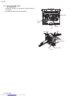
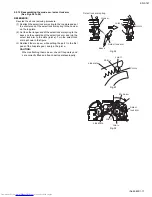
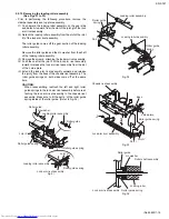
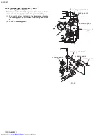
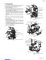
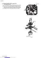
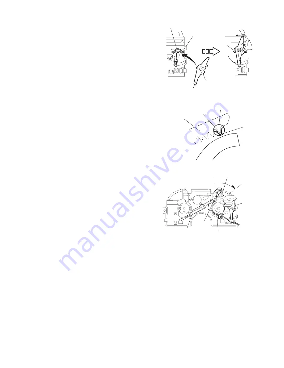
2.2.12 Reassembling the mode sw. / select lock arm 

(See Figs.24 to 26)

REFERENCE:

Reverse the above removing procedure.
(1) Reattach the select lock arm spring to the top plate and set

the shorter end of the select lock arm spring to the hook w
on the top plate.

(2) Set the other longer end of the select lock arm spring to the

boss x on the underside of the select lock arm, and join the
select lock arm to the slots (joint 

v

). Turn the select lock

arm as shown in the figure.

(3) Reattach the mode sw. while setting the part t to the first

peak of the link plate gear, and join the joint 

u

.

CAUTION:

When reattaching the mode sw., check if the points y and
z are correctly fitted and if each part operates properly.

Fig.24

Fig.25

Fig.26

Select lock arm

Hook w

Boss x

Select lock arm spring

Joint v

Joint v

Link plate

Joint t

Point z

Point y

Select 
lock arm

Mode sw.

Joint t

Joint u

Link plate

Содержание KD-S747

Страница 1: ...APAN LTD No 49822 2003 03 KD S747 CD RECEIVER 49822 2003 03 KD S747 TABLE OF CONTENTS 1 Important Safety Precautions 1 2 2 Disassembly method 1 4 3 Adjustment 1 23 4 Description of major ICs 1 27 COMPACT DIGITAL AUDIO Area Suffix EE Russian Fedeation ...

Страница 2: ...utions Burrs formed during molding may be left over on some parts of the chassis Therefore pay attention to such burrs in the case of preforming repair of this system Please use enough caution not to see the beam directly or touch it in case of an adjustment or operation check ...

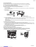
Страница 3: ...ode in the optical pickup The tester s internal power source can easily destroy the laser diode 1 3 Handling the traverse unit optical pickup 1 Do not subject the traverse unit optical pickup to strong shocks as it is a sensitive complex unit 2 Cut off the shorted part of the flexible cable using nippers etc after replacing the optical pickup For specific details refer to the replacement procedure...

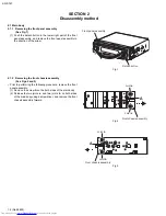
Страница 4: ...1 2 1 2 Removing the front chassis assembly See Figs 2 and 3 Prior to performing the following procedure remove the front panel assembly 1 Remove the screw A on the both sides of the main body 2 Release the two joints a and two joints b on both sides of the main body using a screwdriver and remove the front chassis assembly forward Fig 2 Fig 3 Front panel assembly Detach button Joint a Joint a Fro...

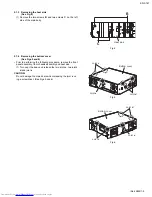
Страница 5: ...6 Prior to performing the following procedure remove the front panel assembly front chassis assembly and heat sink 1 Turn over the body and release the two joints c two joints d and joint e CAUTION Do not damage the main board when releasing the joint e us ing a screwdriver See Figs 5 and 6 Fig 5 Fig 6 B C Heat sink Joint c Joint d Joint e Bottom cover Joint d Joint c Joint e Bottom cover ...

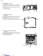
Страница 6: ...orming the following procedure remove the front panel assembly front chassis assembly heat sink bottom cover and rear bracket 1 Remove the two screws G attaching the main board 2 Disconnect connector CN501 and remove the main board Fig 8 2 1 7 Removing the CD mechanism assembly See Fig 9 Prior to performing the following procedure remove the front panel assembly front chassis assembly heat sink bo...

Страница 7: ...ng the following procedure remove the front panel assembly 1 Remove the four screws J on the back side of the front panel assembly 2 Release the twelve joints f 3 Take out the front board Fig 10 Fig 11 Fig 12 J J J Joint f Joint f Rear cover Front panel Joint f Joint f Joint f Front board ...

Страница 8: ... 1 Removing the top cover See Figs 1 and 2 1 Remove the two screws A on the both side of the body 2 Lift the front side of the top cover and move the top cover backward to release the two joints a Fig 1 Fig 2 A A A Joints a Top cover Joints a Top cover ...

Страница 9: ...nector board 2 Solder the short circuit point on the connector board 3 Disconnect the flexible wire from the pickup 4 Move the connector board in the direction of the arrow to release the two joints b 5 Unsolder the wire on the connector board if necessary CAUTION Unsolder the short circuit point after reassembling Fig 3 Fig 4 Fig 5 B Connector board Pickup Short circuit point Joints b Wires Picku...

Страница 10: ... DET switch See Figs 6 and 7 1 Extend the two tabs c of the feed sw holder and pull out the switch 2 Unsolder the DET switch wire if necessary Fig 6 Fig 7 Connector board DET switch Pickup DET switch Tab c Tab c DET switch wire Feed sw holder ...

Страница 11: ...ng the chassis unit to the frame CAUTION The shape of the suspension spring L and R are dif ferent Handle them with care When reassembling make sure that the three shafts on the underside of the chassis unit are inserted to the dampers certainly Fig 8 Fig 9 Suspension spring L Suspension spring L Suspension spring R Suspension spring R Chassis unit Frame Chassis unit Frame Shafts Shaft Damper Damp...

Страница 12: ...procedure remove the top cover 1 Remove the clamper arm spring 2 Move the clamper assembly in the direction of the arrow to release the two joints d Fig 10 Fig 11 Clamper arm spring Chassis rivet assembly Joint d Joint d Clamper assembly Clamper arm spring Clamper assembly Joint d Joint d Chassis rivet assembly ...

Страница 13: ...Remove the screw C and move the loading feed motor assembly in the direction of the arrow to remove it from the chassis rivet assembly 2 Disconnect the wire from the loading feed motor assembly if necessary CAUTION When reassembling connect the wire from the loading feed motor assembly to the flame as shown in Fig 12 Fig 12 Fig 13 Loading feed motor assembly Loading feed motor assembly C ...

Страница 14: ...crew F 2 Reattach the feed sw holder to the feed rack while setting the joint g to the slot of the feed rack and setting the part f of the feed rack to the switch of the feed sw holder correct ly 3 As the feed sw holder is temporarily attached to the pickup unit set to the gear of the joint g and to the bending part of the chassis joint h at a time CAUTION Make sure that the part i on the undersid...

Страница 15: ...t the slot of the chassis rivet assembly respectively and join the joint k at a time Fig 19 Fig 20 2 2 10 Removing the top plate assembly See Fig 21 Prior to performing the following procedure remove the top cover connector board chassis unit and clamper assembly 1 Remove the screw H 2 Move the top plate assembly in the direction of the arrow to release the two joints r 3 Unsolder the wire marked ...

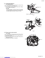
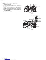
Страница 16: ...he direction of the arrow to release the joint u 2 Unsolder the wire of the mode sw marked s if necessary 3 Turn the select lock arm in the direction of the arrow to re lease the two joints v 4 The select lock arm spring comes off the select lock arm at the same time Fig 22 Fig 23 Mode sw Select lock arm Joint t Link plate Joint u s Top plate Top plate Select lock arm Select lock arm spring Select...
Страница 17: ...x on the underside of the select lock arm and join the select lock arm to the slots joint v Turn the select lock arm as shown in the figure 3 Reattach the mode sw while setting the part t to the first peak of the link plate gear and join the joint u CAUTION When reattaching the mode sw check if the points y and z are correctly fitted and if each part operates properly Fig 24 Fig 25 Fig 26 Select l...
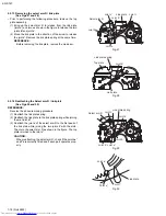
Страница 18: ...igs 29 and 30 REFERENCE Reverse the above removing procedure 1 Reattach the link plate spring 2 Reattach the link plate to the link plate spring while joining them at joint d 3 Reattach the joint a of the select arm R to the first peak of the link plate while joining the two joints b with the slots Then turn the select arm R as shown in the figure The top plate is joined to the joint c CAUTION Whe...

Страница 19: ...late 5 Extend the lock arm rivet assembly outward and release the joint j from the boss of the chassis rivet assembly The roller guide springs on both sides come off at the same time CAUTION When reassembling reattach the left and right roller guide springs to the lock arm rivet assembly before reat taching the lock arm rivet assembly to the chassis rivet assembly Make sure to fit the part k of th...

Страница 20: ...ver chassis unit pickup unit and top plate assembly 1 Remove the screw K attaching the loading gear bracket The loading gear 6 and 7 come off the loading gear brack et 2 Pull out the loading gear 5 Fig 35 Fig 36 K Loading gear bracket Loading gear 6 Loading gear 5 Loading gear 3 K Loading gear bracket Loading gear 6 Loading gear 5 Loading gear 7 ...

Страница 21: ...ff 7 Remove the loading gear 1 8 Move the change plate rivet assembly in the direction of the arrow to release from the three shafts of the chassis rivet assembly upward See Fig 38 9 Detach the loading gear plate rivet assembly from the shaft of the chassis rivet assembly upward while releasing the joint p See Figs 38 and 40 10 Pull out the loading gear 4 Fig 37 Fig 38 Fig 39 Fig 40 Slot m Slot m ...

Страница 22: ...lowing procedure remove the top cover connector board chassis unit and clamper assembly 1 Remove the two screws L attaching the spindle motor as sembly through the slot of the turn table on top of the body 2 Unsolder the wire on the connector board if necessary Fig 41 Fig 42 L Turn table L Turn table Spindle motor ...

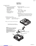
Страница 23: ...be used for AM and FM For FM dummy load there is a loss of 6dB between SSG output and antenna input The loss of 6dB need not be considered since direct reading of figures are applied in this working standard Standard volume position Balance and Bass Treble volume lndication 0 Loudness OFF Frequency Band FM1 FM2 87 5MHz 108 0MHz FM3 65 0MHz 74 0MHz MW 522kHz 1620kHz LW 144kHz 279kHz The cardboard i...

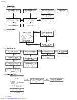
Страница 24: ...s in the vicinity of IC581 pins H K Check the pickup and its connections NO YES YES Does the S search waveform appear at IC581 pins H and I 4V Is the disk rotated Does the RF signal appear at TP1 Is 4V present between IC581 pins 1 and 2 Check the spindle motor and its wiring Is 4V present at IC521 pin x Check the vicinity of IC581 Check IC501 and IC521 YES NO NO NO NO NO YES YES YES Check the circ...

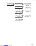
Страница 25: ...d output from both channels L R Check the vicinity of the Q981 audio power supply NO NO NO NO YES YES YES YES YES Check IC521 and its peripheral circuits Is the audio signal including sampling output components output to IC521 pins and during Is the audio signal output at IC101 pins 1 and7during playback NO Check IC101 and its peripheral circuits Check the muting circuit Normal ...

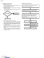
Страница 26: ... whole optical block do not touch the semi fixed resistor If the laser power is lower than the specified value the laser diode is almost worn out and the laser pickup should be re placed If the semi fixed resistor is adjusted while the pickup is functioning normally the laser pickup may be damaged due to excessive current 3 4 Replacement of laser pickup Is RF output 1 0 0 35Vp p Replace it NO YES ...

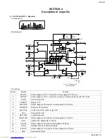
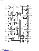
Страница 27: ...CTRL L ANT output OFF H ANT output ON 8 VCC Connected to VCC 9 BATT DET Low battery detect 10 AUDIO OUT Output voltage is 9V when M or H level applied to CTRL pin 11 CTRL L BIAS OFF M BIAS ON H CD ON 12 CD OUT Output voltage is 8V when H level applied to CTRL pin 13 ILM AJ Adjustment pin for ILM output voltage 14 ILM OUT Output voltage is 10V when M or H level applied to CTRL pin 15 GND Connected ...

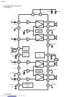
Страница 28: ... Vcc 1 2 Vcc 3 4 OUT 1 OUT 1 PWR GND1 OUT 2 OUT 2 PWR GND2 R F IN 3 IN 4 PRE GND ON TIME C Muting ON Time Control Circuit Protective circuit Protective circuit Mute circuit Ripple Filter Stand by Switch N C 0 22 F 2200 F 0 022 F 0 22 F TAB 5V ST ON 47 F 0 22 F 0 22 F 22 F Mute 10K 3 3 F OUT 3 OUT 3 Low Level Mute ON PWR GND3 OUT 4 OUT 4 PWR GND4 ...

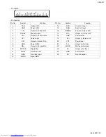
Страница 29: ...3 FR Outpur for front Rch 16 ONTIME Power on time control 4 STDBY Stand by input 17 RL Output for rear Lch 5 FR Output for front Rch 18 GND Power GND 6 VP1 Power input 19 RL Output for rear Lch 7 RR Output for rear Rch 20 VP3 Power input 8 GND Power GND 21 FL Output for front 9 RR Output for rear Rch 22 MUTE Muting control input 10 RIPPLE Ripple filter 23 FL Output for front 11 RRIN Rear Rch input...

Страница 30: ...D VIN1 SW MUTE VREFIN VCCS 3 3VREG REGIN VIN2G VIN2 VIN3G VIN3 FR VIN1 A VIN1 A VCCP1 VO VO VO2 VO2 VO3 VO3 VO4 VO4 VCCP2 VIN4 VIN4G FR H L VIN1_SW H OP AMP_A L OP AMP_B 33k 11k Signal system power supply All outputs ON OFF H ON L OFF MUTE Level shift Level shift Power system GND Signal system power supply 3 3VREG External PTP Tr Power system GND Level shift Level shift 33k 11k 11k 33k 33k 11k ...

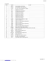
Страница 31: ...upply 13 VIN4 Input pin for channel 4 14 VIN4G Input pin for channel 4 for gain adjustment 15 VIN3 Input pin for channel 3 16 VIN3G Input pin for channel 3 for gain adjustment 17 VIN2 Input pin for channel 2 18 VIN2G Input pin for channel 2 for gain adjustment 19 REGIN External PNP transistor base connection 20 3 3VREG 3 3VREG output pin external PNP transistor collector connection 21 VCCS Signal ...

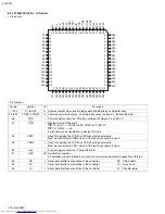
Страница 32: ...e externally Must be connected to VDD1 when a 1 2 bias drive scheme is used 60 Vss Power supply connection Connect to GND 61 OSC I O Oscillator connection An oscillator circuit is formed by connecting an external resistor and capacitor at this pin 62 CE I Serial data interface connection to the controller CE Chip enable 63 CL I Serial data interface connection to the controller CL Sync clock 64 DI...

Страница 33: ...KD S747 No 49822 1 33 4 5 NJM4565M WE IC571 CD L P F 4 6 IC PST600M G W IC702 System reset 8 7 6 5 4 3 2 1 V B OUTPUT B INPUT B INPUT A INPUT A INPUT A OUTPUT V IN Vout GND 1 3 2 OP1 Co1 ...

Страница 34: ... 20k 3k 180k 240k 240k 15pF 15pF 40pF 40pF 10pF 60k 60k 22k 22k 94k 94k 14k 50k 20k 20k 20k 40k 50k PEAK 15k 40k 2k 1 75k 1 3V 2k 1k 180k 3k 12k 12k 20k 40k 30k 10pF 50 A BOTTOM PEAK K 1 x0 5 x2 x0 5 x2 PIN SEL APC SW TEB TE BAL RFGC AGC Gian TEB TE BAL VCTRLPIN VCC APC ON 50 12dB Normal mode 0dB HiZ APC ON 0 6dB Normal mode 0dB GND APC OFF LDO H 50 0dB CD RW mode 12dB ...

Страница 35: ...king search system 12 RFDC O RF signal peak detection output pin 13 GVSW I AGC FE TE amp gain change pin 14 VRO O Reference voltage VRO output pin VRO 1 2VCC When VCC 3 3V 15 FEO O Focus error signal generation amp output pin 16 FEN I Focus error signal generation amp negative phase input pin 17 RFRP O Signal amp output pin for track count Combining RFRP signal and TEO signal with TC94A14F FA conf...

Страница 36: ...t pin L for L channel and H for R channel Output polarity can be inverted by command 3 AOUT O Audio data output pin MSB first or LSB first selectable by command 4 DOUT O Digital data output pin Outputs up to double speed playback 5 IPF O Correction flag output pin When set to H AOUT output cannot be corrected by C2 correction processing 6 VDD3 Digital 3 3V power supply voltage pin 7 VSS3 Digital G...

Страница 37: ...H output with UHS H 39 AVDD3 Analog 3 3V power supply voltage pin 40 FMO O Feed equalizer output pin 41 DMO O Disc equalizer output pin 42 VSS3 Digital GND pin 43 VDD3 Digital 3 3V power supply voltage pin 44 TESIN I Test input pin Normally fixed to L 45 XVSS3 System clock oscillator GND pin 46 XI I System clock oscillator input pin 47 XO O System clock oscillator output pin 48 XVDD3 System clock ...

Страница 38: ...PORT Vdd Vcc Pin No Symbol I O Function Pin No Symbol I O Function 1 XOUT O Crystal oscillator pin 13 IFC I IF signal input 2 OSC Non connect 14 VDD Power pins for digital block 3 CE I Chip enable input 15 FMIN I FM band local signal input 4 DI I Serial data input 16 AMIN I AM band local signal input 5 CK I Clock input 17 DGND Connect to GND for digital circuit 6 DOUT O Serial data output 18 FMCP ...

Страница 39: ...eft front 5 TL I Treble control capacitor left channel or input from an external equalizer 6 B2L Bass control capacitor left channel or output to an external equalizer 7 B1L Bass control capacitor left channel 8 IVL I Input volume 1 left control part 9 ILL I Input loudness left control part 10 QSL O Output source selector left channel 11 IDL Not used 12 MUTE Not used 13 ICL I Input C left source 1...

Страница 40: ... 17 no use O output L 18 PS2 I power save2 H means STOP mode 19 22 no use O output L 23 AVDD A D converter power supply 24 AVREF0 A D reference voltage 25 VOLÇP I volume encoder pulse input 1 26 VOLÇQ I volume encoder pulse input 2 27 KEY0 I key input 0 28 KEY1 I key input 1 29 KEY2 I key input 2 30 LEVEL I level meter input 31 no use I Input 32 SM I S DMETER input 33 AVSS GND 34 35 no use O outpu...

Страница 41: ...phone muting detection input Active level can be selected H or L in PSM 71 no use O output L 72 VSS GND 73 no use I output L 74 PS1 I POWER SAVE1 Çk ACC off 75 POWER O POWER ON OFF control output H power on 76 CD ON O CD power supply control output H CD power on 77 MUTING O muting output L muting on 78 80 no use O output L 81 VDD maicon power supply 82 no use O output L 83 VOL DA O data output for...

Страница 42: ... No 49822 AV MULTIMEDIA COMPANY MOBILE ENTERTAINMENT CATEGORY 10 1 1chome Ohwatari machi Maebashi city 371 8543 Japan VICTOR COMPANY OF JAPAN LIMITED 200303WPC Printed in Japan KD S747 ...

Страница 43: ...CH 2003 03 COPYRIGHT 2003 VICTOR COMPANY OF JAPAN LTD KD S747 KD S747 Area suffix EE Russian Federation KD S747 COMPACT DIGITAL AUDIO Contents Block diagram Standard schematic diagrams Printed circuit boards 2 1 2 2 2 5 7 CD ROM No SML200303 ...

Страница 44: ...ft over on some parts of the chassis Therefore pay attention to such burrs in the case of preforming repair of this system Safety precaution Please use enough caution not to see the beam directly or touch it in case of an adjustment or operation check ...

Страница 45: ...EY0 KEY1 KEY2 ENC1 ENC2 IC601 LCD DRIVER LCD1 CN701 TU1 FM AM TUNER IC701 CPU IC161 E VOL FM AM MONO SM SD ST SEEK STOP IC301 POWER AMP IC901 REGULATOR SPK BATTERY EACH BLOCK L CH R CH OUTLF OUTRF OUTLR OUTRR REAR L REAR R CD L CD R J301 LINE OUT LF LF RF RF LR LR RR RR COM1 COM2 COM3 S1 S50 LCDCE LCDDA LCDCL VOLDA VOLCL RDSSCK RDSDA J1 ANT SW1 SW2 PSW LM MSW CD RW FEED FEED SPINDLE SPINDLE VF1 VF...

Страница 46: ... UN2111 X 22 16 0 022 0 01 560P 47P 82P 2 2 50 100P 47k 1 50 1 50 UN2211 X 2SD1781K QR X 4 7 50 4 7 50 4 7 50 1 50 IC PST600M G W BR24L16F W X 7P 1 50 10P 2 2K 10 22K 1K 0 01 1 50 QNN0519 001 10K 47K 0 01 47K 1K 2 2 50 10 100 47K 100K 10K 100K 100 22K 100K 47K 220 0 1 0 047 10K 120P 47k UN2111 X 0 2 2K 0 47P 1SS355 X 10 2 2K 2 2K 4 7 50 180K 22K 0 047 2SD1781K QR X 12K 1 50 1 50 2SD601A R X 10K 47...

Страница 47: ...15 0 01 0 0027 0 01 0 033 0 470P 470P 8 2K 0 033 0 0 0 047 0 047 100 6 3 100 6 3 10K 1A3G T1 820 0 01 100 100 10 100 6 3 0 0068 0 18K 0 330K 82K 330K 82K 150 100 6 3 150 4 7K 8 2K 18K 120P 10P 6 8K 4 7 25 15K 10P 0 22 22 4 7 25 1 5K 1M 33K 12K 33K 33K 12K 120P 120P 0 01 1 5K 1 5K 0 047 0 047 0 047 0 047 4 7 4 7 4 7 100 6 3 100 10 1 50 22K 22K 22K 22K 0 001 0 01 56K 0 1 0 1 47P 0 047 100 100 0 047 ...

Страница 48: ... SV4 470 VMC0335 001 LC75823W 10 6 3 0 0 022 10K 10K 10K QLD0254 001 1 2K 820 1 8K 2 7K 820 820 2 7K 1 8K 1 2K 820 3 9K 820 1 2K 1 8K 1K 820 UDZS5 1B X 47K QSW0863 002 47K 0 015 0 015 0 47K UN2211 X 1K SML 310LT MN X 1K 820 10K 820 510 510 510 820 1K 820 330 510 820 330 820 0 012 51K 680P 820 820 820 UDZS5 1B X UDZS6 2B X 0 NSPW310BS B2RS 430 2SB624 4 X NSPW310BS B2RS 430 0 KEY0 KEY1 S32 KEY2 S17 ...

Страница 49: ...592 C593 C594 C595 C596 C709 C710 C712 C781 C782 C784 C901 C903 C904 C905 C906 C907 C910 C911 C913 C915 CN501 CN701 CN901 D71 D161 D171 D321 D341 D561 D901 IC31 IC71 IC161 IC301 IC501 IC521 IC561 IC571 IC701 IC702 IC801 IC901 J1 J301 J801 L1 L521 L522 L523 L524 L701 L901 Q53 Q71 Q72 Q73 Q74 Q321 Q331 Q341 Q351 Q501 Q561 R11 R32 R33 R42 R43 R56 R58 R74 R75 R76 R77 R161 R171 R301 R321 R323 R331 R333...

Страница 50: ...D708 D709 D781 D782 D783 D891 D892 D901 D902 D903 D904 IC301 IC901 J1 J301 J801 L1 L521 L522 L523 L524 L701 L901 LM MSW Q1 Q2 Q3 Q4 Q5 Q6 Q7 Q31 Q51 Q52 Q241 Q501 Q521 Q522 Q561 Q781 Q782 Q783 Q891 Q901 Q902 R1 R2 R3 R4 R5 R6 R7 R8 R9 R10 R31 R34 R35 R36 R37 R38 R39 R40 R41 R44 R51 R52 R53 R54 R55 R57 R59 R71 R72 R73 R81 R82 R91 R92 R162 R163 R164 R165 R166 R167 R168 R172 R173 R174 R175 R176 R177 ...

Страница 51: ... R605 R606 R607 R608 R609 R610 R631 R646 R647 S601 S602 S603 S604 S605 S606 S607 S608 S609 S610 S611 S612 S613 S614 S615 S616 S617 S618 C601 C602 C603 C612 C613 C614 CJ601 D641 D642 D644 D645 D731 D732 JS690 IC601 IC602 Q641 Q642 R612 R613 R614 R615 R616 R632 R633 R634 R635 R636 R637 R638 R639 R640 R641 R642 R643 R644 R645 R648 R649 R651 R653 R654 R655 R656 R657 R658 R659 R660 R662 R663 R670 R671 ...

Страница 52: ...KD S747 VICTOR COMPANY OF JAPAN LIMITED AV MULTIMEDIA COMPANY 10 1 1Chome Ohwatari machi Maebashi city 371 8543 Japan No 49822SCH Printed in Japan 2003 03 ...

Страница 53: ...le as service parts Contents KD S747 Area suffix EE Russian Federation Exploded view of general assembly and parts list Block No M1 3 2 CD mechanism assembly and parts list Block No MP 3 4 Electrical parts list Block No 01 02 3 6 Packing materials and accessories parts list Block No M3 M5 3 10 ...

Страница 54: ...ts list 6 6 46 2 1 6 5 4 37 41 43 44 42 A B 36 36 35 40 22 23 21 19 20 18 33 25 24 27 34 32 30 28 31 29 26 54 10 10 7 16 15 17 12 13 14 11 47 53 8 9 50 51 9 49 48 9 7 3 52 Block No M M M 1 45 39 38 Main board Main board 8 Front Front board board LCD1 LCD1 ...

Страница 55: ...E30816 002A SEL BUTTON 23 FSYH4036 053 SHEET 24 GE30817 001A RIM LENS 25 GE30811 002A PUSH BUTTON 26 GE20143 001A PRESET BUTTON 27 GE30814 007A D FUNC BTN DOW 28 GE30807 001A DETACH BUTTON 29 FSKW3002 012 COMP SPRING 30 GE30818 001A NAVI BUTTON 31 GE30819 001A NAVI BASE 32 GE40127 002A COMP SPRING 33 GE30813 001A D FUNC BTN UP 34 GE30803 001A EJECT BUTTON 35 GE10058 001A REAR COVER 36 VKZ4777 001 ...

Страница 56: ... C C D D B a a B TN 2001 1011 111 2 111 37 27 32 23 13 15 99 28 98 83 12 86 121 16 17 124 4 125 1 111 3 3 71 111 93 111 91 92 113 88 89 82 87 20 18 115 90 32 30 38 114 11 85 25 73 111 33 34 74 72 35 26 31 22 36 116 29 112 19 61 24 112 62 21 38 76 95 96 14 97 100 123 81 94 77 75 74 73 84 94 101 100 122 93 75 83 ...

Страница 57: ...T SUSPENSION SP L 61 69011614T PICKUP OPT 725 62 64180406T DET SW ESE22 71 303210301T CONN PWB ASS Y 72 30321002T MODE SW 73 30321003T LOAD MOTOR WIRE 74 30321005T MODE SW WIRE 75 30321009T SL WIRE 76 30321011T WIRE HOLDER 77 19501403T WIRE CLUMPER 81 303211301T ROLLER SHAFT AS 82 303211501T L GEAR PLATE RV 83 303211302T LOADING PLATE A 84 303211502T LOCK ARM RV ASS 85 303211303T L F MOTOR ASS Y 8...

Страница 58: ... C42 NCB31HK 103X C CAPACITOR 0 01uF 50V K C43 QFV61HJ 473Z MF CAPACITOR 0 047uF 50V J C44 NCB31EK 333X C CAPACITOR 0 033uF 25V K C45 NCB31HK 682X C CAPACITOR 6800pF 50V K C46 NCB31HK 103X C CAPACITOR 0 01uF 50V K C47 NCB31HK 103X C CAPACITOR 0 01uF 50V K C48 NCB31EK 473X C CAPACITOR 0 047uF 25V K C50 NCS31HJ 101X C CAPACITOR 100pF 50V J C55 NCS31HJ 331X C CAPACITOR 330pF 50V J C81 NCB31EK 123X C ...

Страница 59: ...PACITOR 8pF 50V J C704 NDC31HJ 270X C CAPACITOR 27pF 50V J C705 NDC31HJ 270X C CAPACITOR 27pF 50V J Symbol No Part No Part Name Description Local C706 NDC31HJ 220X C CAPACITOR 22pF 50V J C707 NCB31EK 473X C CAPACITOR 0 047uF 25V K C708 NCB31EK 103X C CAPACITOR 0 01uF 25V K C709 QEKJ0JM 476Z E CAPACITOR 47uF 6 3V M C710 NCB31EK 473X C CAPACITOR 0 047uF 25V K C711 NCB31HK 103X C CAPACITOR 0 01uF 50V...

Страница 60: ... R593 NRSA63J 123X MG RESISTOR 12kΩ 1 16W J R594 NRSA63J 151X MG RESISTOR 150Ω 1 16W J R595 NRSA63J 0R0X MG RESISTOR 0Ω 1 16W J R596 NRSA63J 223X MG RESISTOR 22kΩ 1 16W J R597 NRSA63J 223X MG RESISTOR 22kΩ 1 16W J Symbol No Part No Part Name Description Local R598 NRSA63J 0R0X MG RESISTOR 0Ω 1 16W J R703 NRSA63J 473X MG RESISTOR 47kΩ 1 16W J R704 NRSA63J 473X MG RESISTOR 47kΩ 1 16W J R706 NRSA63J ...

Страница 61: ... 16W J R631 NRSA02J 821X MG RESISTOR 820Ω 1 10W J R632 NRSA02J 102X MG RESISTOR 1kΩ 1 10W J R633 NRSA02J 102X MG RESISTOR 1kΩ 1 10W J R634 NRSA02J 821X MG RESISTOR 820Ω 1 10W J R635 NRSA02J 821X MG RESISTOR 820Ω 1 10W J R636 NRSA02J 821X MG RESISTOR 820Ω 1 10W J R637 NRSA02J 821X MG RESISTOR 820Ω 1 10W J R638 NRSA02J 331X MG RESISTOR 330Ω 1 10W J R639 NRSA02J 331X MG RESISTOR 330Ω 1 10W J R640 NRS...

Страница 62: ...KD S747 3 10 Packing materials and accessories parts list Block No M M M 3 Block No M M M 5 P1 A1 A3 P6 P7 P7 P5 A12 A11 A4 P4 P3 A10 A13 P2 KIT A5 A9 4 ...

Страница 63: ...ARTON P7 GE10070 001A EPS CUSHION Symbol No Part No Part Name Description Local A1 GET0138 001A INST BOOK ENG RUS A2 GET0138 002A INSTALL MANUAL ENG RUS A3 BT 54013 5 WARRANTY CARD A4 LV40978 001A CAUTION SHEET A5 VKZ4027 202 PLUG NUT A6 VKH4871 001SS MOUNT BOLT A7 VKZ4328 001 LOCK NUT A8 WNS5000Z WASHER A9 GE40130 001A HOOK x2 A10 FSJB3002 00C HARD CASE A11 GE20137 003A MOUNTING SLEEVE A12 GE2013...

Отзывы: