background image

1-12

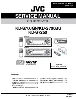
KD-S700GN/KD-S700BU
KD-S7250

Power ON

 Set Function to CD

Play

Jump to the first track

TOC readout

Tracking loop closed

Disc rotates

Disc inserted

YES

YES

Laser emitted

Pickup feeds to the inner area

Focus search

RF signal eye-pattern
opens

RF signal eye-pattern
remains closed

"No disc"

display

• When correctly focused

 Focus Servo Loop ON

• When the laser diode correctly 

emits

Microprocessor

commands

Rough Servo Mode

CLV Servo Mode
 (ProgramArea)

CLV Servo Mode
 (Lead-In Area; 
   Digital: 0)

• RF signal

Flow of functional operation until TOC read

• When the pickup correctly moves 

to the inner area of the disc

TERMINAL

Microprocessor

commands

FMO
TC9490FA "40"

FEED MOTOR
+TERMINAL
IC561 "6"

REST SW

• When the disc correctly rotates 

Tracking Servo Loop ON

Servo CLV

Rough

Servo

Acceleration

Acceleration

Microprocessor
commands

Spindle
motor (-) 
IC561 "4"

0.5 Sec 0.5 Sec

3.3v

FEO

TA2147F

1.6V

TC9490FA"38"

"1"

3.3V

1.6V

"41"

Содержание KD-S700BU

Страница 1: ...0 KD S700GN KD S700BU KD S7250 Area Suffix J Northern America Contents Safety precaution Preventing static electricity Disassembly method Adjustment method Flow of functional operation unit TOC read 1 2 1 3 1 4 1 11 1 12 Maintenance of laser pickup Replacement of laser pickup Discription of major ICs 1 14 1 14 1 15 ...

Страница 2: ... may be left over on some parts of the chassis Therefore pay attention to such burrs in the case of preforming repair of this system Safety precaution Please use enough caution not to see the beam directly or touch it in case of an adjustment or operation check ...

Страница 3: ...fter replacement return the shorted parts to their original condition Refer to the text 2 Do not use a tester to check the condition of the laser diode in the optical pickup The tester s internal power source can easily destroy the laser diode 4 Handling the traverse unit optical pickup 1 Do not subject the traverse unit optical pickup to strong shocks as it is a sensitive complex unit 2 Cut off t...

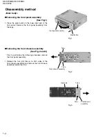
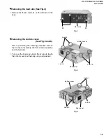
Страница 4: ...orming the following procedure remove the front panel assembly Release the four joint tabs a on both sides of the front chassis assembly and remove the front chassis assembly toward the front 1 Removing the front chassis assembly See Fig 2 and 3 Disassembly method Main body Fig 1 Fig 2 Fig 3 Front panel assembly Eject button Tab a Tab a Front chassis assembly Front chassis assembly Heat sink Tab a...

Страница 5: ...edure remove the front panel assembly the front chassis assembly and the heat sink Turn over the body and unjoint the five joints b with the bottom cover and the body using a screwdriver 1 Removing the bottom cover See Fig 5 and 6 Fig 4 Fig 5 Fig 6 Heat sink A A Joints b Joints b Joint b Joints b Joints b Joint b Bottom cover Bottom cover Rear panel Rear panel ...

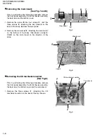
Страница 6: ...n board on the bottom of the body Disconnect connector CN501 on the main board in the direction of the arrow 1 2 Removing the main board See Fig 7 and 8 Prior to performing the following procedure remove the front panel assembly the front chassis assembly the heat sink the bottom cover and the main board Remove the three screws F attaching the CD mechanism section on the back of the top chassis 1 ...

Страница 7: ... on the back of the front panel assembly Unjoint the twelve joints c with the front panel and the rear cover Remove the control switch board on the back of the front panel 1 2 3 Removing the control switch board See Fig 10 to 12 Fig 10 Fig 11 Fig 12 G G G G Rear cover Joints c Joints c Front panel Rear cover Front panel Control switch board Joints c Joints c ...

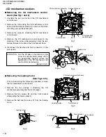
Страница 8: ...e entire pickup unit to the appropriate position where the flexible wire of the CD mechanism unit can be disconnected easily Refer to Fig 2 ATTENTION Prior to performing the following procedure remove the CD mechanism control board Remove the two springs f attaching the CD mechanism assembly and the front bracket Remove the two screws B and the front bracket while pulling the flame outward Remove ...

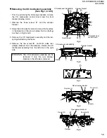
Страница 9: ...Remove the two screws E and both sides rear damper brackets from the dampers Detach the CD mechanism assembly from the left side to the right side 1 2 3 4 Removing the CD mechanism assembly See Fig 1 6 to 9 The CD mechanism assembly can be removed if only the rear damper bracket on the left side is removed ATTENTION Fig 6 Fig 7 Fig 8 Fig 9 Rear damper bracket Fix arm R Damper D D Damper bracket CD...

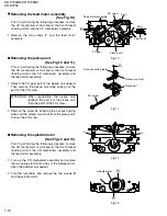
Страница 10: ...nd the pickup mount nut from the pickup unit Pull out the FD screw 2 Removing the pickup unit See Fig 10 and 11 When reattaching the pickup unit reattach the part j of the pickup unit then the part i of the FD screw ATTENTION Prior to performing the following procedure remove the CD mechanism control board the front bracket loading motor the CD mechanism assembly and the feed motor assembly Turn u...

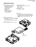
Страница 11: ...DC14 4V 11V 16V allowance Load impedance 4 4 to 8 allowance Line out Level impeadance 2 0V 20k load full scale Output Impedance 1k How to connect the extension cable for adjusting Dummy load Exclusive dummy load should be used for AM and FM For FM dummy load there is a loss of 6dB between SSG output and antenna input The loss of 6dB need not be considered since direct reading of figures are applie...

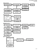
Страница 12: ...e laser diode correctly emits Microprocessor commands Rough Servo Mode CLV Servo Mode ProgramArea CLV Servo Mode Lead In Area Digital 0 RF signal Flow of functional operation until TOC read When the pickup correctly moves to the inner area of the disc TERMINAL Microprocessor commands FMO TC9490FA 40 FEED MOTOR TERMINAL IC561 6 REST SW When the disc correctly rotates Tracking Servo Loop ON Servo CL...

Страница 13: ...C561 pins 15 18 Check the pickup and its connections NO YES YES YES Does the S search waveform appear at IC561 pins 8 and 9 Is the disk rotated Does the RF signal appear at TP1 Is 4V present at IC561 pins 4 and 5 Check the spindle motor and its wiring Is 3 3V present at IC521 pin 41 Check the vicinity of IC581 Check IC501 and IC521 YES NO NO NO NO NO YES YES YES Check the circuits in the vicinity ...

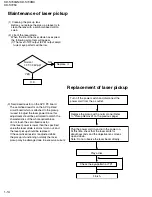
Страница 14: ...wer Since this adjustment should be performed to match the characteristics of the whole optical block do not touch the semi fixed resistor If the laser power is lower than the specified value the laser diode is almost worn out and the laser pickup should be replaced If the semi fixed resistor is adjusted while the pickup is functioning normally the laser pickup may be damaged due to excessive curr...

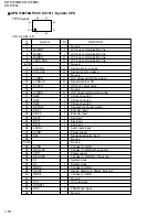
Страница 15: ...ANT CTRL VCC BATT DET AUDIO OUT CTRL CD OUT ILM AJ ILM OUT GND Output voltage is VCC 1 V when M or H level applied to CTRL pin Output voltage is VCC 1 V when M or H level to CTRL pin and H level to ANT CTRL Connected to ACC Regular 5 7V Output voltage is 5V when M or H level applied to CTRL pin Output for ACC detector L ANT output OFF H ANT output ON Connected to VCC Low battery detect Output volt...

Страница 16: ...communication line JVC bus communication line JVC bus communication line JVC bus communication line No use Serial data for volume Serial clock for volume No use LCD driver serial data output Serial data for LCD JVC bus output select No use LCD driver communication line CD mech switch CD mech switch CD mech switch Traverse mech rest switch Encoder input Encoder input Key input Key input Key input A...

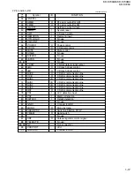
Страница 17: ... for AM PLL error output for FM Setting to write for flash System reset CD mech switch Remocon input No use No use Power control CD power control Mute control No use No use No use No use CD RW detect signal output CD mech driver control CD mech driver control CD LSI communication line CD LSI communication line CD LSI communication line CD LSI communication line CD LSI communication line CD LSI com...

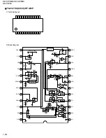
Страница 18: ...0k 180k 40pF 40pF 3k 3k 12k 12k 15k 50 A 10pF 20 A 40k 20k 20k 20k 50k PEAK 15k 10pF 40k 60 A 1 3V BOTTOM PEAK 40k 30k 13 GVSW VRO FEO FEN RFRP RFRPIN RFGO RFGC AGCIN RFO RFN GND 14 15 16 17 18 19 20 21 22 23 24 12 RFDC TEO TEN TEBC SEL LDO MDI TNI TPI FPI FNI Vcc 11 10 9 8 7 6 5 4 3 2 1 TA2147F X IC501 RF AMP 1 Terminal layout 2 Block diagram ...

Страница 19: ...ference voltage VRO output pin VRO 1 2 Vcc when Vcc 3 3V Focus error signal generation amp output pin Focus error signal generation amp negative phase input pin Signal amp output pin for track count Combining RFRP signal TEO signal with TC9490F FA configures tracking search system Signal generation amp input pin for track count RF signal amplitude adjustment amp output pin RF amplitude adjustment ...

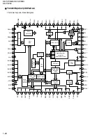
Страница 20: ...5 44 43 42 41 40 39 38 37 36 35 34 33 1 2 3 4 5 6 7 8 9 10 11 12 13 14 15 16 17 18 19 20 21 22 23 24 25 26 27 28 29 30 31 32 64 63 62 61 60 59 58 57 56 55 54 53 52 51 50 49 BCK LRCK AOUT DOUT IPF V DD3 V SS3 SBOK CLCK DATA SFSY SBSY HSO UHSO PV DD3 PDO VXDD3 XO XI XV SS3 TEIN V DD3 V SS3 DMO FMO AV DD3 SEL TEBC RFGC V REF TRO FOO DVSS3 RO DVDD3 DVR LO DVSS3 ZDET VSS5 BUS0 BUS1 BUS2 BUS3 BUCK CCE R...

Страница 21: ...LCK phase difference signal output pin TMAX detection result output pin Inverted input pin for PLL LPF amp Output oin for PLL LPF amp PLL only VREF pin VCO filter pin Analog GND pin DAC output pin for data slice level generation RF signal input pin Zin selectable by command Analog 3 3V power supply voltage pin RFRP signal center level input pin RFRP signal zero cross input pin RF ripple signal inp...

Страница 22: ... 3 3V power supply voltage pin DA converter GND pin R channel data forward output pin DA converter 3 3V power supply pin Reference voltage pin L channel data forward output pin DA converter GND pin 1 bit DA converter zero data detection flag output pin Microcontroller interface GND pin Microcontroller interface data I O pins Microcontroller interface clock input pin Microcontroller interface chip ...

Страница 23: ...utput Pin CH1 Rear Output Pin CH1 Front Output Pin CH1 Bass Filter Setting Pin CH1 Bass Filter Setting Pin CH2 Bass Filter Setting Pin CH2 Bass Filter Setting Pin CH2 Treble Filter Setting Pin CH1 Treble Filter Setting Pin CH2 Treble Input Pin CH2 BBE II Signal Output Pin CH2 Output MIX Amplifier Inverse Input Pin A2 B2 C2 D2 FIL GND SI SC VCC OUTR2 OUTF2 OUTR1 OUTF1 BOUT1 BNF1 BOUT2 BNF2 TNF2 TNF...

Страница 24: ...D1 OUT 2 OUT 2 PWR GND2 R F IN 3 IN 4 PRE GND ON TIME C Muting ON Time Control Circuit Protective circuit Protective circuit Mute circuit Ripple Filter Stand by Switch N C 0 22 F 2200 F 0 022 F 0 22 F TAB 5V ST ON 47 F 0 22 F 0 22 F 22 F Mute 10K 3 3 F OUT 3 OUT 3 Low Level Mute ON PWR GND3 OUT 4 OUT 4 PWR GND4 LA4743K IC302 Power AMP 1 Block diagram ...

Страница 25: ... 19 20 21 22 23 24 25 Symbol Pin No Function Header of IC Power GND Outpur for front Rch Stand by input Output for front Rch Power input Output for rear Rch Power GND Output for rear Rch Ripple filter Rear Rch input Front Rch input Signal GND Front Lch input Rear Lch input Power on time control Output for rear Lch Power GND Output for rear Lch Power input Output for front Muting control input Outp...

Страница 26: ...nal CH4 output terminal CH3 output terminal CH3 output terminal CH2 output terminal CH2 output terminal CH1 output terminal CH1 output terminal CH1 2 3 4 power supplies CH1 input terminal CH1 input terminal for gain adjustment VCC2 VO5 VO5 VO4 VO4 VO3 VO3 VO2 VO2 VO1 VO1 VCC1 VIN1 VIN1G 15 16 17 18 19 20 21 22 23 24 25 26 27 28 CH2 input terminal CH2 input terminal for gain adjustment CH3 input te...

Страница 27: ... Load Circuit 1 Sample as Load Circuit 1 Note CL includes probe and jig capacitance 1k 1k S1 CL Input Note H High level L Low level X Irrelevant Z Off High impedance State a 3 state input Output C L H H A X L H Y Z H L 1 2 3 4 5 6 7 1C 1A 1Y 2C 2A 2Y GND VU 4C 4A 4Y 3C 3A 3Y 14 13 12 11 10 9 8 HD74HC126FP X IC801 Buffer 1 Terminal layout 2 Block diagram 3 Pin function ...

Страница 28: ...tput pins Common driver output pins Power supply Ground pin Oscillation Input Output pin Chip enable pin Synchronization clock Transfer data pin Used for the 2 3 bias voltage when the bias voltages are provided externally Connect to VDD2 when 1 2 bias is used Used for 1 3 bias voltage when the bias voltages are provided externally Connect to VDD1 when 1 2 bias used Display OFF control input pin Wh...

Страница 29: ...6 5 4 3 2 1 V B OUTPUT B INPUT B INPUT A INPUT A INPUT A OUTPUT V NJM4565M WE IC571 Ope amp RPM6938 SV4 IC602 Remote sensor Vcc Vcc Comp AGC AMP PD Detector BPF fo trimming circuit I V conversion magnetic shield Rout GND 22k 1 Block diagram ...

Страница 30: ...MOCON IC601 LCD DRIVER LCD1 CJ961 TU1 FM AM TUNER IC701 MICON IC161 E VOL FM AM FMOSC IFC AGC S METER SD ST MONO S METER AMEO FMEO IC302 POWER AMP IC901 REGULATOR SPK BATTERY EACH BLOCK TU LCH TU RCH CD L CD R CJ302 LINE OUT LF RF LR RR LM0 LM1 COM1 COM2 COM3 S1 S50 LCD_CO LCD_CLK LCD_SO ANT CDON PS2 CJ1 ANT Block diagram LD MD SW1 SW4 REST FEED CD L CD R DMO FMO FOD TRO RF GC RF RFRP TE SEL TEB R...

Страница 31: ...16 UN2111 QAN0009 001Z HA13164A 470p 1k 1 4W 10k 2SD1048 6 7 X 47k 2 2 25 CRS03 W 2 2 25 2 2 25 1000p 0 1 2 2 50 10 16 10 16 0 022 1SS133 1SS133 1SS133 1SS133 100p 4 7k 100p 100p 100p 100p 100p 100p 100p UN2211 X 2SD1048 6 7 X 2SD1048 6 7 X 2SD1048 6 7 X 0 4 7k UN2211 X 51k 1k 47k 470 UN2111 0 01 4 7u 2 2k 1k 1k UN2211 X 0 0 22 47k 47k 10k 330 UN2211 X 47k QAU0257 001 22k 47k 2 2k 100 VMC0334 001 ...

Страница 32: ... 01 0 0027 0 01 0 033 0 470p 470p 8 2k 1 10W 0 033 0 0 0 047 0 047 10k 2SB1322 820 0 01 100 47 6 3 100 10 0 0068 10k 15k 82k 82k 150k 82k 150k 82k 22 10 150 5 6k 820p 820p 4 7 25 6 8k 15k 820p 4 7 25 10p 10p UN2111 6 8k 820p UN2211 10k 10k 12k 33k 33k 12k 100 10 120p 120p 0 01 QGB2027M1 26S 47 6 3 47u 22k 22k 20k 1 10W 0 047 100 100 0 047 100 100 0 047 100 10 0 01 100 10 4 7k 4 7k 4 7k 4 7k 1 50 1...

Страница 33: ...k 10 6 3 1SS335 X 1SS335 X QSW0793 001 RPM6938 SV4 10k 470 UDZS5 1B X PT6523LQ 0 022 3 9k 2 2k 51k 0 022 680p 10k 10k 10k 1 2k 820 1 8k 2 7k 820 820 3 9k 2 7k 1 8k 1 2k 1 2k 1 8k 2 7k 2 2k 820 VCM0335 001 390 1 8W 510 4 7 6 3 0 012 510 100 510 0 022 510 820 UDZS6 2B X 390 1 8W 820 LCD CE LCD DA LCD CL LCD_SO LCD_CLK LCD_CO Key0 Key1 REMOCON Key2 ENC1 R5V KEY0 KEY1 KEY2 S17 S18 OSC ENC2 GND S19 S20...

Страница 34: ... D903 D905 D906 D907 D908 D976 IC161 IC302 IC501 IC521 IC561 IC571 IC701 IC801 IC901 L1 L521 L522 L523 L524 L701 L702 L901 Q321 Q331 Q341 Q351 Q501 Q561 R31 R41 R161 R171 R183 R184 R185 R186 R187 R188 R193 R194 R195 R196 R197 R198 R221 R305 R306 R307 R308 R316 R325 R331 R335 R341 R345 R355 R533 R571 R574 R581 R584 R685 R686 R704 R718 R720 R722 R727 R802 R901 R902 R903 R907 R908 R909 R961 TU1 X521 ...

Страница 35: ... Q963 Q964 Q976 Q977 R1 R2 R3 R5 R8 R9 R10 R21 R22 R23 R24 R25 R26 R27 R32 R33 R34 R42 R43 R81 R82 R83 R84 R162 R163 R172 R173 R175 R176 R181 R182 R191 R192 R201 R211 R241 R242 R243 R244 R245 R246 R247 R248 R249 R321 R322 R332 R342 R351 R352 R501 R502 R503 R504 R505 R506 R507 R508 R509 R510 R511 R512 R513 R514 R515 R516 R517 R521 R522 R523 R524 R525 R526 R527 R528 R529 R530 R531 R532 R534 R535 R53...

Страница 36: ...VICTOR COMPANY OF JAPAN LIMITED MOBILE ELECTRONICS DIVISION PERSONAL MOBILE NETWORK BUSINESS UNIT 10 1 1Chome Ohwatari machi Maebashi city 371 8543 Japan No 49670 200112 KD S700GN KD S700BU KD S7250 ...

Отзывы: