


KD-S670
1-19
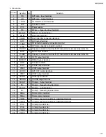
2.Terminal layout
3.Pin function
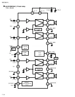
LA4743B
TAB
GND
OUTRR-
STBY
OUTRR+
VCC1/2
OUTRF-
GND
OUTRF+
RIPPLE
INRF
INRR
SGND
INLR
INLF
ONTIME
OUTLF+
GND
OUTLF-
VCC3/4
OUTLR+
MUTE
OUTLR-
GND
NC
1
2
3
4
5
6
7
8
9
10
11
12
13
14
15
16
17
18
19
20
21
22
23
24
25
Symbol
Pin No.
Function
Header of IC
Power GND
Output(-) for front Rch
Stand by input
Output (+) for front Rch
Power input
Output (-) for rear Rch
Power GND
Output (+) for rear Rch
Ripple filter
Rear Rch input
Front Rch input
Signal GND
Front Lch input
Rear Lch input
Power on time control
Output (+) for rear Lch
Power GND
Output (-) for rear Lch
Power input
Output (+) for front
Muting control input
Output (-) for front
Power GND
Non connection
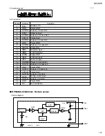
RPM6938-SV4(IC602) : Remote sensor
Vcc
Vcc
Comp
AGC
AMP
PD
Detector
BPF
fo
trimming
circuit
I/V
conversion
magnetic
shield
Rout
GND
22k
1.Block diagram
Содержание KD-S670
Страница 34: ...KD S670 2 7 M E M O ...
Страница 45: ...KD S670 3 11 M E M O ...


