1
2
3
5
4
A
B
C
D
E
F
G
H
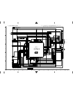
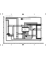
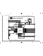
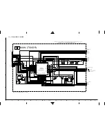
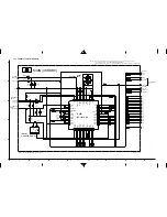
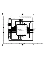
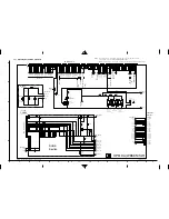
AUDIO AD/DA SCHEMATIC DIAGRAM
4.5
4-12
4-11
EM_AU/R
EM_AU/L
R2104
AIDAT2
R2103
REG_3V
GND
DOBCK2
L2101
C2107
C2110
PWDA2
MD_DEM1
R2105
IC2101
DOLRCK2
C2108
R2102
R2101
C2106
C2105
DODAT2
DOMCK2
PWAD2
C2109
MD_AU/R
R2106
C2103
C2104
MD_AU/L
C2102
C2101
R2107
R2110
R2112
R2108
R2113
R2111
MP_MUTE
R2109
C2112
C2111
C2113
C2114
Q2101
10
µ
10
4.7
3.3k
0.1
470
470
0.0022
0.0022
0.1
3.3k
1
1
1
1
560k
0
Ω
0
Ω
560k
0
Ω
3.3k
/6.3
/6.3
VCOM
AINR
AINL
VSS
VDD
DEM0
DEM1
SDT
O
SDTI
LRCK
MCLK
SCLK
PW
AD
PWD
A
A
OUTL
A
OUTR
AK4550VT-X
UMX18N-W
T
T
TO
DSC
∗
∗
∗
∗
∗
∗
0 1
TO
REG
TO
MAIN AUDIO
TO
SYSCON-CPU
y30174001a_rev0
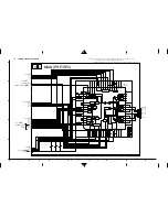
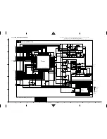
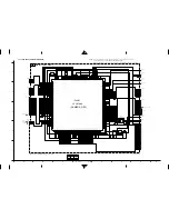
MAIN (AUDIO AD/DA)
NOTE : The parts with marked (
∗
) is not used.
When ordering parts, be sure to order according to the Part Number indicated in the Parts List.
For the destination of each signal and further line connections that are cut off from
this diagram, refer to "4.1 BOARD INTERCONNECTIONS".
NOTES :

