
MX-KA7
1-32
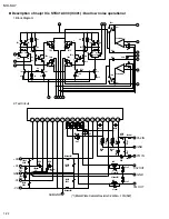
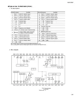
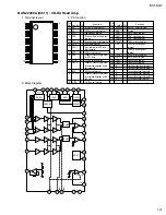
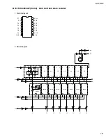
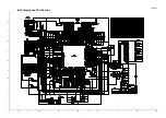
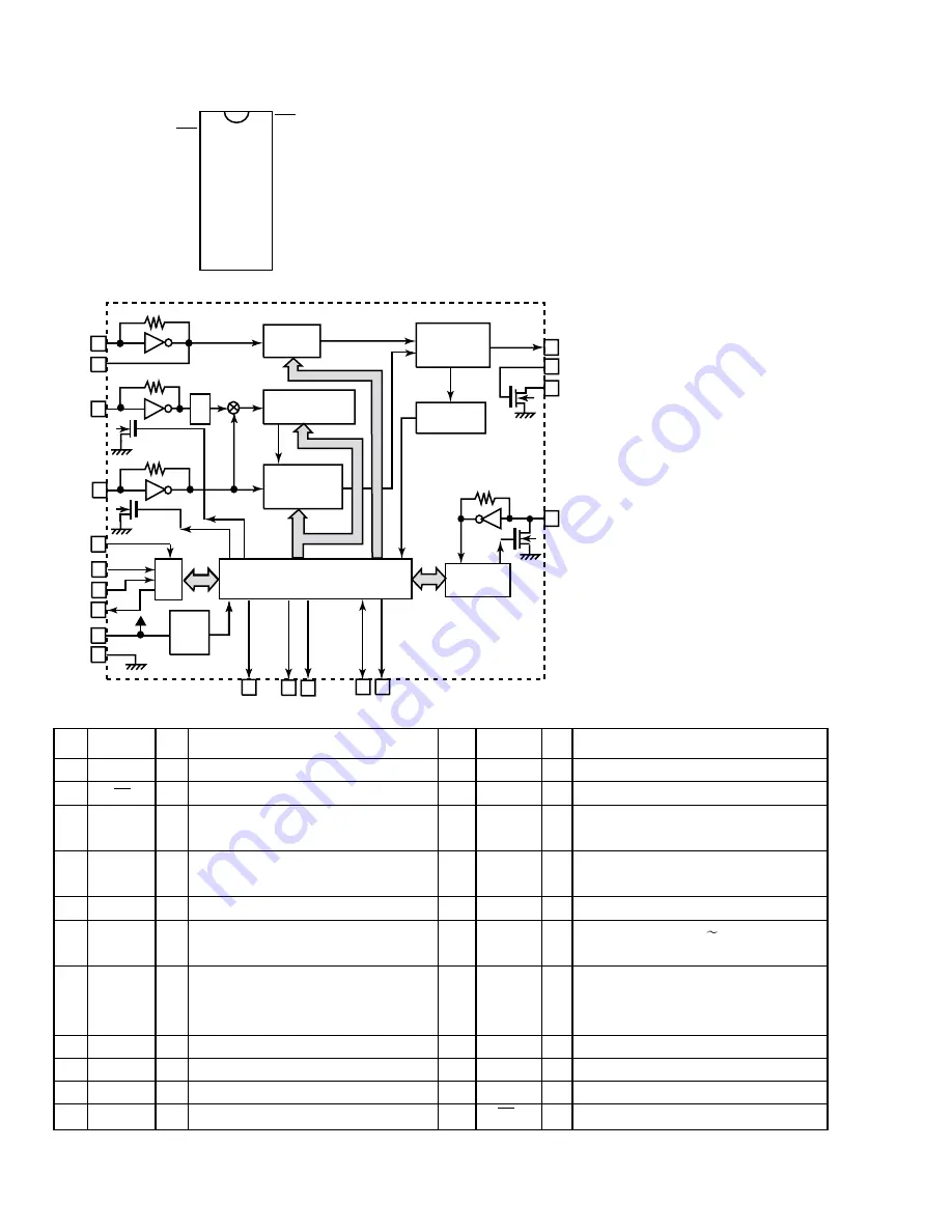
1.Terminal layout
1
2
3
4
5
6
7
8
9
10
11
22
21
20
19
18
17
16
15
14
13
12
XTI
FM
CE
DI
CLOCK
DO
VCOSTOP
AM/FM
LW
MW
SDIN
XT
GND
LPFI
LPFO
PD
VCC
FMIN
AMIN
NC
IFCNT
IFIN
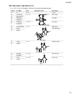
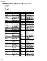
Pin
No.
1
2
3
4
5
6
7
8
9
10
11
Pin
No.
12
13
14
15
16
17
18
19
20
21
22
Symbol
XTI
FM
CE
DI
CLOCK
DO
VCOSTOP
AM/FM
NC
NC
SDIN
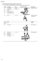
Symbol
IFIN
IFCNT
NC
AMIN
FMIN
VCC
PD
LPFO
LPFI
GND
XT
Function
X'tal oscillator connect (75KHz)
LOW:FM mode
When data output/input for 4pin(input) and
6pin(output): H
Input for receive the serial data from
controller
Sync signal input use
Data output for Controller
Output port
"Low": MW mode
Open state after the power on reset
Input/output port
Input/output port
Data input/output
Function
IF counter signal input
IF signal output
Not use
AM Local OSC signal output
FM Local OSC signal input
Power supply(VDD=4.5 5.5V)
When power ON:Reset circuit move
PLL charge pump output(H: Local OSC
frequency Height than Reference frequency.
L: Low Agreement: Height impedance)
Output for active lowpassfilter of PLL
Input for active lowpassfilter of PLL
Connected to GND
X'tal oscillator(75KHz)
I/O
I
O
I
I
I
O
O
O
-
-
I/O
I/O
I
O
-
I
I
-
O
O
I
-
I
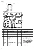
Reference
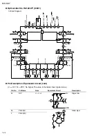
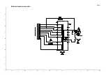
Driver
Phase
Detector
Charge Pump
Unlock
Detector
Universal
Counter
Swallow Counter
1/16,1/17 4bit
12bit
Programmable
DriverS
Swallow Counter
1/16,1/17 4bit
Data Shift Register & Latch
Power
on
Reset
C
2
B
I/F
1/2
7
8
2
11
13
21
17
6
5
4
3
15
16
22
1
18
19
20
12
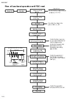
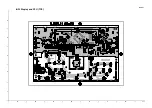
2. Block diagram
3. Pin function
LC72136N (IC2) : PLL Frequency synthesizer
Содержание CA-MXKA7
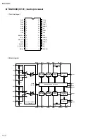
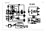
Страница 23: ...MX KA7 1 23 1 Pin descriptions 2 Block diagram Optical disc ICs BA5936S IC621 ...
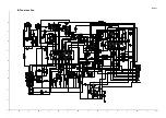
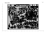
Страница 35: ...A B C D E F G 1 2 3 4 5 2 1 MX KA7 n Tuner section ...
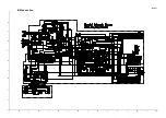
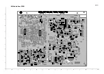
Страница 36: ...A B C D E F G 1 2 3 4 5 2 2 n Main section MX KA7 ...
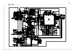
Страница 37: ...A B C D E F G 1 2 3 4 5 2 3 MX KA7 n CD section ...
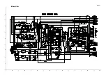
Страница 38: ...A B C D E F G 1 2 3 4 5 2 4 MX KA7 n Amplifier ...
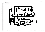
Страница 39: ...A B C D E F G 1 2 3 4 5 2 5 MX KA7 n FL Display and CPU Control ...
Страница 40: ...A B C D E F G 1 2 3 4 5 2 6 MX KA7 n Power transformer section ...
Страница 41: ...A B C D E F G 1 2 3 4 5 2 7 MX KA7 n Block diagram ...
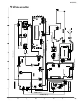
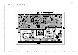
Страница 42: ...A B C D E F G 1 2 3 4 5 2 8 MX KA7 n Wiring diagram ...
Страница 43: ...A B C D E F G 1 2 3 4 5 2 9 MX KA7 n Main top PWB ...
Страница 44: ...A B C D E F G 1 2 3 4 5 2 10 MX KA7 n Main bottom PWB ...
Страница 45: ...A B C D E F G 1 2 3 4 5 2 11 MX KA7 n FL Display and CPU TOP ...
Страница 46: ...A B C D E F G 1 2 3 4 5 2 12 MX KA7 n FL Display and CPU BOTTOM ...
Страница 47: ...A B C D E F G 1 2 3 4 5 2 13 MX KA7 n Power Amp PWB ...
Страница 48: ...A B C D E F G 1 2 3 4 5 2 14 MX KA7 n Power trans PWB ...
Страница 59: ...3 11 MEMO ...


