background image

User Guide 003

2

UG003.0

September 17, 2014

Submit Document Feedback

Recommended Equipment

• DC power supply with minimum 15V/25A sourcing capacity
• Electronic load capable of sinking current up to 50A
• Digital multimeters (DMMs)
• Oscilloscope with higher than 100MHz bandwidth

Functional Description

The ISL8272MEVAL1Z provides all circuitry required to evaluate 
the features of the ISL8272M. A majority of the features of the 
ISL8272M, such as compensation-free ChargeMode™ control, 
soft-start delay and ramp times, supply sequencing, and voltage 
margining are available on this evaluation board. For sequencing 
evaluation, the board can be connected to any Intersil digital 
module evaluation board that supports the DDC bus. 

Figures 1

 and 

2

 show the board images of the ISL8272MEVAL1Z 

evaluation board. 

Quick Start Guide

Pin-Strap Option

ISL8272MEVAL1Z can be configured in pin-strap mode with 
standard 1% 0603 resistors. PMBus interface is not required to 
evaluate ISL8272M in pin-strap mode. Output voltage (V

OUT

), 

switching frequency (f

SW

), soft-start/stop delay and ramp time, 

input undervoltage protection (UVLO) threshold, ASCR gain and 
residual, and device PMBus address can be changed by 
populating recommended resistors at placeholders provided in 
the evaluation board. By default, the evaluation board operates 
in pin-strap mode and regulates at V

OUT

 = 1.2V, f

SW

 = 421kHz, 

soft-start/stop delay time = 5ms, soft-start/stop ramp 
time = -5ms, UVLO = 4.5V, ASCR gain = 200, ASCR residual = 90 
and PMBus address = 28h. Follow these steps to evaluate 
ISL8272M in pin-strap mode.

1. Set ENABLE switch to “DISABLE”.
2. Connect Load to VOUT lug connectors (J7-J8 and J9-J10).

3. Connect power supply to VIN connectors (J5 and J6). Make 

sure power supply is not enabled when making connection. 

4. Turn power supply on.
5. Set ENABLE switch to “ENABLE”.
6. Measure 1.2V VOUT at probe point labeled “VOUT 

REGULATION MONITOR” (J11).

7. Observe switching frequency of 421kHz at probe points 

labeled “PHASE1” (TP10) and “PHASE2” (TP11). 

8. To measure the module efficiency, connect the multimeter 

voltage probes at probe points labeled “VIN” (TP1), “GND” 
(TP2) and “VOUT” (TP12).

9. To change VOUT, disconnect board from the setup and 

populate a 1% standard 0603 resistor at RVSET placeholder 
location on bottom layer. Refer to the “Output Voltage 
Resistor Settings” table in the 

ISL8272M

 datasheet for 

recommended values. By default, VOUT_MAX is set to 110% 
of VOUT set by pin-strap resistor. 

10. To change switching frequency, disconnect board from the 

setup and populate a 1% standard 0603 resistor at RFSET 
placeholder location on bottom layer. Refer to the “Switching 
Frequency Resistor Settings” table in the 

ISL8272M


datasheet for recommended values.

11. To change soft-start/stop delay and ramp time, disconnect 

board from the setup and populate a 1% standard 0603 
resistor at R6 placeholder location on bottom layer. Refer to 
the “Soft Start/Stop Resistor Settings” table in the 

ISL8272M


datasheet for recommended values.

12. To change UVLO, disconnect board from the setup and 

populate a 1% standard 0603 resistor at R6 placeholder 
location on bottom layer. Refer to the “UVLO Resistor Settings” 
table in the 

ISL8272M

 datasheet for recommended values. 

Notice that the UVLO programming shares the same pin with 
soft-start/stop programming.

13. To change ASCR gain and residual, disconnect board from the 

setup and populate a 1% standard 0603 resistor at R7 
placeholder location on bottom layer. Refer to the “ASCR 

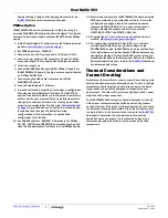
FIGURE 2. BOTTOM SIDE

RESISTOR PLACEHOLDERS

Содержание ISL8272MEVAL1Z

Страница 1: ...s References ISL8272M datasheet Key Features VIN range of 4 5V to 14V VOUT adjustable from 0 6V to 5V Programmable VOUT margining input and output UVP OVP IOUT limit OTP UTP soft start stop sequencing and external synchronization Monitor VIN VOUT IOUT temperature duty cycle switching frequency and faults ChargeMode control tunable with PMBus Mechanical switch for enable and power good LED indicato...

Страница 2: ...9 J10 3 Connect power supply to VIN connectors J5 and J6 Make sure power supply is not enabled when making connection 4 Turn power supply on 5 Set ENABLE switch to ENABLE 6 Measure 1 2V VOUT at probe point labeled VOUT REGULATION MONITOR J11 7 Observe switching frequency of 421kHz at probe points labeled PHASE1 TP10 and PHASE2 TP11 8 To measure the module efficiency connect the multimeter voltage ...

Страница 3: ...be used from the PowerNavigator software to allow PMBus Enable 11 Monitor and configure the ISL8272MEVAL1Z board using the PMBus commands in the evaluation software To store the configuration changes disable the module and use the command STORE_USER_ALL To restore factory default settings disable the module and use the command RESTORE_FACTORY and STORE_USER_ALL 12 PowerNavigator tutorial videos ar...

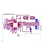
Страница 4: ...11 C21 100UF 100UF C13 0 1UF C1 TP7 C18 470UF TP2 1 2 J11 TP8 DNP R5 100UF C14 SW1 1 2 3 C24 470UF TP6 22UF C4 VDRV1 VDRV1 EN NC VOUT VSENP VSENN VOUT NC NC PG ASCR VDRV VDRV SS UVLO CS MGN PGND PGND PGND VCC V25 VR5 VR6 SWD2 SWD1 SW1 PGND SW2 PGND PGND PGND PGND PGND VMON SGND SGND SGND SGND SGND DDC SYNC SA PGND PGND VIN VIN VIN VR VR55 SCL SDA SALRT NC NC NC VSET VDD U1 ISL8272MIRZ PAD6 M14 K16...

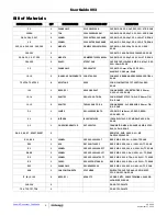
Страница 5: ...2HLF CONN HEADER 1X2 RETENTIVE 2 54mm 0 230 x 0 120 ROHS J2 J4 2 SAMTEC SSQ 103 02 T D RA CONN SOCKET STRIP TH 2x3 2 54mm TIN R A ROHS J1 J3 2 SAMTEC TSW 103 08 T D RA CONN HEADER 2x3 BRKAWY 2 54mm TIN R A ROHS D1 1 LUMEX SSL LXA3025IGC TR LED SMD 3x2 5mm 4P RED GREEN 12 20MCD 2V U1 1 INTERSIL ISL8272MAIRZ IC 50A DIGITAL DC DC MODULE 42P HDA ROHS Q1 1 ON SEMICONDUCTOR 2N7002LT1G TRANSISTOR MOS N C...

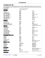
Страница 6: ...able and no retry ISENSE_CONFIG 0x05 256ns Blanking time Mid Range Other Faults OT_FAULT_LIMIT 0xebe8 125 C OT_FAULT_RESPONSE 0x80 Disable and no retry OT_WARN_LIMIT 0xeb70 110 C UT_WARN_LIMIT 0xdc40 30 C UT_FAULT_LIMIT 0xe530 45 C UT_FAULT_RESPONSE 0x80 Disable and no retry VIN_OV_FAULT_LIMIT 0xd380 14 V VIN_OV_FAULT_RESPONSE 0x80 Disable and no retry VIN_OV_WARN_LIMIT 0xd353 13 3 V VIN_UV_WARN_L...

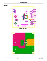
Страница 7: ...User Guide 003 7 UG003 0 September 17 2014 Submit Document Feedback Layout FIGURE 3 SILKSCREEN TOP FIGURE 4 TOP LAYER COMPONENT SIDE ...

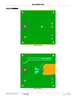
Страница 8: ...User Guide 003 8 UG003 0 September 17 2014 Submit Document Feedback FIGURE 5 LAYER 2 FIGURE 6 LAYER 3 Layout Continued ...

Страница 9: ...User Guide 003 9 UG003 0 September 17 2014 Submit Document Feedback FIGURE 7 LAYER 4 FIGURE 8 LAYER 5 Layout Continued ...

Страница 10: ...User Guide 003 10 UG003 0 September 17 2014 Submit Document Feedback FIGURE 9 BOTTOM LAYER SOLDER SIDE FIGURE 10 SILKSCREEN BOTTOM Layout Continued ...

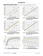
Страница 11: ... vs SWITCHING FREQUENCY AT VIN 12V IOUT 50A FOR VARIOUS OUTPUT VOLTAGES 55 50 45 40 35 30 25 20 15 10 5 0 0 5 10 15 20 25 30 35 40 45 50 55 ACTUAL OUTPUT CURRENT A MEASURED OUTPUT CURRENT A 300kHz 533kHz 421kHz 800kHz 55 50 45 40 35 30 25 20 15 10 5 0 0 5 10 15 20 25 30 35 40 45 50 55 ACTUAL OUTPUT CURRENT A MEASURED OUTPUT CURRENT A 45 C 65 C 25 C 300kHz 533kHz 421kHz 800kHz 55 50 45 40 35 30 25 ...

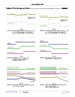
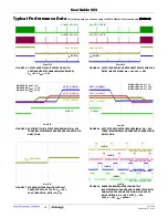
Страница 12: ...IN 12V VOUT 1 2V TOFF_DELAY 5ms TOFF_FALL 5ms FIGURE 21 OUTPUT SHORT CIRCUIT PROTECTION AT VIN 12V VOUT 1 2V fSW 533kHz FIGURE 22 OUTPUT OVERVOLTAGE PROTECTION AT VIN 12V VOUT 1 2V fSW 533kHz VOUT_OV_FAULT_LIMIT 1 38V Typical Performance Data The following data was acquired using a ISL8272MEVAL1Z evaluation board Continued VOUT 50mV DIV IOUT 25A DIV 20µs DIV ASCR GAIN 550 RESIDUAL 100 VOUT 50mV DI...

Страница 13: ...mV µs FIGURE 28 PHASE SPREADING INTERLEAVING TWO ISL8272MEVAL1Z BOARDS ARE CONNECTED IN DAISY CHAIN MODULE 1 RAIL POSITION 0 MODULE 2 RAIL POSITION 4 VIN 12V VOUT_1 1 2V VOUT_2 3 3V fSW 421kHz Typical Performance Data The following data was acquired using a ISL8272MEVAL1Z evaluation board Continued PHASE1 10V DIV PHASE2 10V DIV VOUT 1V DIV IIN 5A DIV 50ms DIV PHASE1 10V DIV PHASE2 10V DIV VOUT 1V ...

Страница 14: ...ief is current before proceeding For information regarding Intersil Corporation and its products see www intersil com UG003 0 September 17 2014 Submit Document Feedback FIGURE 29 THERMAL IMAGE AT VIN 12V VOUT 1V IOUT 50A fSW 300kHz TA 25 C NO AIRFLOW FIGURE 30 THERMAL IMAGE AT VIN 14V VOUT 5V IOUT 50A fSW 533kHz TA 25 C NO AIRFLOW Typical Performance Data The following data was acquired using a IS...

Страница 15: ...Mouser Electronics Authorized Distributor Click to View Pricing Inventory Delivery Lifecycle Information Intersil ISL8272MEVAL1Z ...

Отзывы: