User Guide 026
UG026.1
February 3, 2017
2
Test Steps
1. Ensure that the circuit is correctly connected to the supply and
loads prior to applying any power.
2. Connect the bias supply to VIN. Plus terminal to VIN
(TP1) and
negative return to PGND (TP2).
3. Connect the output load to VO
(TP3), and the negative return
to PGND (TP4).
4. Turn on the power supply.
5. Verify the output voltage is 1.8V for VOUT
.
Functional Description
The ISL800xxxDEMO1Z boards provide a simple platform to
evaluate performance of the ISL80020, ISL80020A, ISL80015,
and ISL80015A.
These devices are highly efficient, monolithic, synchronous
step-down DC/DC converters that can deliver up to 1.5A or 2A of
continuous output current from a 2.7V to 5.5V input supply. They
use peak current mode control architecture to allow very low duty
cycle operation. The devices operate at 1MHz or 2MHz switching
frequency, thereby providing superior transient response and
allowing for the use of a small inductor.
These devices are configured in PWM (Pulse Width Modulation)
for fast transient response, which helps reduce the output noise
and RF interference.
PCB Layout Guidelines
The PCB layout is a very important converter design step to make
sure the designed converter works well. The power loop is
composed of the output inductor L’s, the output capacitor C
OUT
,
the PHASE’s pins, and the PGND pin. It is necessary to make the
power loop as small as possible and the connecting traces
among them should be direct, short, and wide. The switching
node of the converter, the PHASE pins, and the traces connected
to the node are very noisy. Therefore, keep the voltage feedback
trace away from these noisy traces. The input capacitor should
be placed as close as possible to the VIN pin and the ground of
the input and output capacitors should be connected as closely
as possible. The heat of the IC is mainly dissipated through the
thermal pad. Maximizing the copper area connected to the
thermal pad is preferable. In addition, a solid ground plane is
helpful for better EMI performance. It is recommended to add at
least four vias to the ground connection within the pad for the
best thermal relief.
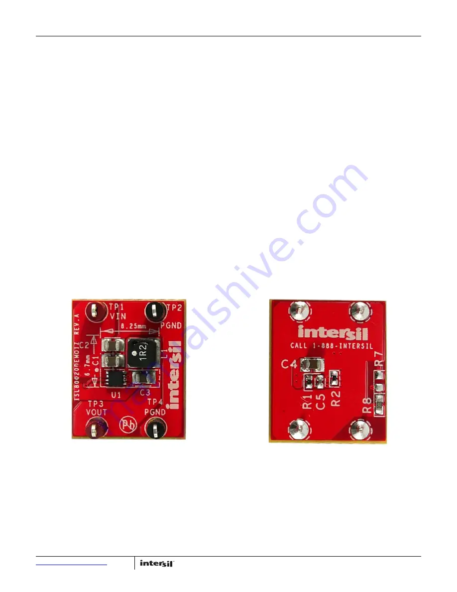
FIGURE 2. ISL80020DEMO1Z TOP SIDE
FIGURE 3. ISL80020DEMO1Z BOTTOM SIDE


