


IRDC3846-P1V2
Confidential
This evaluation board is a preliminary version meant for the engineering evaluation of the IR3846. Based on the results
of the continuing evaluation, this board can evolve and change without notice
AL
4/11/2013
2
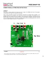
A well reg12V input supply should be connected to VIN+ and VIN-. A maximum of 35A load should
be connected to VOUT+ and VOUT-. The inputs and output connections of the board are listed in Table I.
IR3846 needs only one input supply and internal LDO generates Vcc from Vin. If operation with external Vcc
is required, then R3 should be removed and external Vcc can be applied between Vcc+ and Vcc- pins. Vin
pin and Vcc pins should be shorted together for external Vcc operation by installing a 0 ohm resistor at R4.
The board is configured for remote sensing. If local sense is desired, R18 should be uninstalled and R19
should be installed instead.
External Enable signal can be applied to the board via exposed Enable pad and
R100 should be removed
for this purpose.
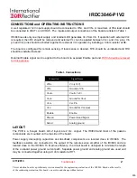
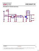
CONNECTIONS and OPERATING INSTRUCTIONS
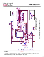
LAYOUT
The PCB is a 6-layer board. All of layers are 2 Oz. copper. The IR3846 and most of the passive
components are mounted on the top side of the board.
Power supply decoupling capacitors and feedback components are located close to IR3846. The
feedback resistors are connected to the output of the remote sense amplifier of the IR3846 and are
located close to the IR3846. To improve efficiency, the circuit board is designed to minimize the length
of the on-board power ground current path. Separate power ground and analog ground are used and
may be connected together using a 0 ohm resistor at R71.
Table I. Connections
Connection
Signal Name
VIN+
Vin (+12V)
VIN-
Ground of Vin
Vout+
Vout(+1.2V)
Vout-
Ground for Vout
Vcc+
Vcc Pin
Vcc-
Ground for Vcc input
Enable
Enable
PGood
Power Good Signal
AGnd
Analog ground