International Rectifier SupIRBuck IR3898 Скачать руководство пользователя страница 7

IRDC3898-P3V3 

8/15/2013 


Confidential 


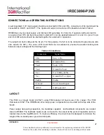
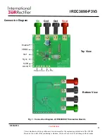
This evaluation board is a preliminary version meant for the engineering evaluation of the  IR3898. 
Based on the results of the continuing evaluation, this board  can evolve and change without notice 
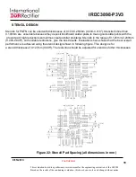
7


 Bill of Materials 

Item  Qty

Part Reference

Value

Description

Manufacturer

Part Number

1

1

C1

330uF

SMD Electrolytic F size 25V 20%

Panasonic

EEV-FK1E331P

2

3

C3 C4 C5 

10uF

1206, 16V, X5R, 20%

TDK

C3216X5R1C106M

3

4

C7 C12 C14 C24

0.1uF

0603, 25V, X7R, 10%

Murata

GRM188R71E104KA01B

4

1

C8

2200pF

0603,50V,X7R

Murata

GRM188R71H222KA01B

5

1

C11

130pF

0603, 50V, NP0, 5%

Murata

GRM1885C1H131JA01D

6

3

C15 C16 C17 

22uF

0805, 6.3V, X5R, 20%

TDK

C2012X5R0J226M 

7

1

C23 

2.2uF

 0603, 16V, X5R, 20%

TDK

C1608X5R1C225M

8

1

C26

5.6nF

 0603, 25V, X7R, 10%

Murata

GRM188R71E562KA01J

9

1

C32

1.0uF

 0603, 25V, X5R, 10%

Murata

GRM188R61E105KA12D

10

1

L1

1.0uH

SMD 7.1x6.5x5mm,4.7mΩ

TDK

SPM6550T-1R0

11

1

R1

2.49K

Thick Film, 0603,1/10W,1%

Panasonic

ERJ-3EKF2491V

12

2

R2 R11

4.42K

Thick Film, 0603,1/10W,1%

Panasonic

ERJ-3EKF4421V

13

2

R3 R12

787

Thick Film, 0603,1/10W,1%

Panasonic

ERJ-3EKF7870V

14

1

R4

75

Thick Film, 0603,1/10W,1%

Panasonic

ERJ-3EKF75R0V

15

1

R6 

20

Thick Film, 0603,1/10W,1%

Panasonic

ERJ-3EKF20R0V

16

1

R9 

23.2K

Thick Film, 0603,1/10W,1%

Panasonic

ERJ-3EKF2322V

17

5

R10 R13 R14 R15 R50

0

Thick Film, 0603,1/10W

Panasonic

ERJ-3GEY0R00V

18

2

R17 R18

49.9K

Thick Film, 0603,1/10W,1%

Panasonic

ERJ-3EKF4992V

19

1

R19

9.09K

Thick Film, 0603,1/10W,1%

Panasonic

ERJ-3EKF9091V

20

1

U1

IR3898

PQFN 4x5mm

IR

IR3898MPBF

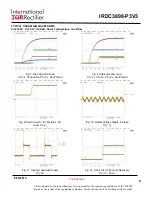
BOM   IRDC3898 Vin-12V   Vout-3.3V/6.0A   Freq-1MHz

Содержание SupIRBuck IR3898

Страница 1: ...nder voltage lockout for proper start up enhanced line load regulation with feed forward external frequency synchronization with smooth clocking internal LDO and pre bias start up Pulse by pulse curre...

Страница 2: ...to be connected to ground use zero ohm resistor for R21 The value of R14 and R28 can be selected to provide the desired tracking ratio between output voltage and the tracking input CONNECTIONS and OP...

Страница 3: ...neering evaluation of the IR3898 Based on the results of the continuing evaluation this board can evolve and change without notice 3 Connection Diagram Vin Gnd Gnd Vout Enable VDDQ Vref Sync S Ctrl AG...

Страница 4: ...nary version meant for the engineering evaluation of the IR3898 Based on the results of the continuing evaluation this board can evolve and change without notice 4 Fig 2 Board Layout Top Layer Fig 3 B...

Страница 5: ...tion board is a preliminary version meant for the engineering evaluation of the IR3898 Based on the results of the continuing evaluation this board can evolve and change without notice 5 Fig 5 Board L...

Страница 6: ...evaluation board is a preliminary version meant for the engineering evaluation of the IR3898 Based on the results of the continuing evaluation this board can evolve and change without notice 6 Fig 6...

Страница 7: ...1 C23 2 2uF 0603 16V X5R 20 TDK C1608X5R1C225M 8 1 C26 5 6nF 0603 25V X7R 10 Murata GRM188R71E562KA01J 9 1 C32 1 0uF 0603 25V X5R 10 Murata GRM188R61E105KA12D 10 1 L1 1 0uH SMD 7 1x6 5x5mm 4 7m TDK S...

Страница 8: ...change without notice 8 TYPICAL OPERATING WAVEFORMS Vin 12 0V Vo 3 3V Io 0 6A Room Temperature no airflow Fig 10 Output Voltage Ripple 6A load Ch1 Vo Fig 11 Inductor node at 6A load Ch1 LX Fig 12 Sho...

Страница 9: ...ant for the engineering evaluation of the IR3898 Based on the results of the continuing evaluation this board can evolve and change without notice 9 TYPICAL OPERATING WAVEFORMS Vin 12 0V Vo 3 3V Io 0...

Страница 10: ...ngineering evaluation of the IR3898 Based on the results of the continuing evaluation this board can evolve and change without notice 10 TYPICAL OPERATING WAVEFORMS Vin 12 0V Vo 3 3V Io 0 6A Room Temp...

Страница 11: ...the IR3898 Based on the results of the continuing evaluation this board can evolve and change without notice 11 TYPICAL OPERATING WAVEFORMS Vin 12 0V Vo 3 3V Io 0 6A Room Temperature no air flow Fig...

Страница 12: ...change without notice 12 Fig 18 Power loss versus load current Fig 17 Efficiency versus load current TYPICAL OPERATING WAVEFORMS Vin 12 0V Vo 3 3V Io 0 6A Room Temperature no air flow 85 86 87 88 89...

Страница 13: ...ng evaluation of the IR3898 Based on the results of the continuing evaluation this board can evolve and change without notice 13 THERMAL IMAGES Vin 12 0V Vo 3 3V Io 0 6A Room Temperature No Air flow F...

Страница 14: ...performance is achieved using the substrate PCB layout as shown in following figures PQFN devices should be placed to an accuracy of 0 050mm on both X and Y axes Self centering behavior is highly depe...

Страница 15: ...MD pads the underlying copper traces should be at least 0 05mm larger on each edge than the Solder Mask window in order to accommodate any layer to layer misalignment i e 0 1mm in X Y However for the...

Страница 16: ...00 0 250mm 0 004 0 010 Stencils thinner than 0 100mm are unsuitable because they deposit insufficient solder paste to make good solder joints with the ground pad high reductions sometimes create simil...

Страница 17: ...s board can evolve and change without notice 17 IR WORLD HEADQUARTERS 233 Kansas St El Segundo California 90245 USA Tel 310 252 7105 TAC Fax 310 252 7903 This product has been designed and qualified f...

Отзывы: