International Rectifier IRDC38063-P1V2 Скачать руководство пользователя страница 2

IRDC38063-P1V2 

3/21/2017 


2


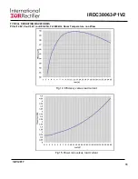
A well reg12V input supply should be connected to PVin+ and PVin-. A maximum of 25A load should 
be connected to VOUT+ and VOUT-. The  inputs and output connections of the board are listed in Table I.  
 
IR38063  needs  only  one  input  supply    and  internal  LDO  generates  Vcc  from  PVin.  Another  internal  LDo 
generates the 1.8V needed by the internal digital circuits. If operation with external Vcc is required, then R25 
should  be  removed  and  external  Vcc  can  be  applied  between  Vcc+  and  Vcc-  pins.  Vin  pin  and  Vcc  pins 
should be shorted together for external Vcc operation by installing R24. For tracking operation R27 should 
be populated with a 0 ohm resistor. 

For normal, non-tracking operation, R27 should not be populated 

and  a 100 kOhm resistor should be connected from the Track_En pin to P1V8.


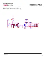
The  board  is  configured  for  remote  sensing.  If  local  sense  is  desired,  R8  should  be  uninstalled  and  R16 
should be installed instead. 
 
I2C/PMBus  communication  is  established  through  the  4  pin  header  which  allows  connection  to  the 
SCL/SDA/SALERT  and  GND  lines  from  the  host/dongle.  For  proper  operation  in  digital  communications 
mode, R35 must always be populated. 


External Enable signal can be applied to the board via exposed Enable pad and 

R18 should be removed for 

this purpose. 


CONNECTIONS and OPERATING INSTRUCTIONS 
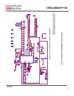
LAYOUT 

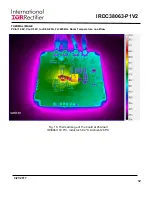
The  PCB  is  a  6-layer  board.  All  of  layers  are  2  Oz.  copper.  The  IR38063  and  most  of  the  passive 
components  are


mounted  on  the  top  side  of  the  board.  Power  supply  decoupling  capacitors  and 

feedback  components  are  located  close  to  IR38063.    The  feedback  resistors  are  connected  to  the 
output of the remote sense amplifier of the IR38063 and are located close to  the IR38063. To improve 
efficiency,  the  circuit  board  is  designed  to  minimize  the  length  of  the  on-board  power  ground  current 

path.


Separate power ground and analog ground are used and may be connected together using a 0 

ohm resistor. 

 
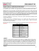
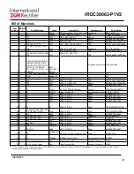
Table I. Connections 

   Connection 

   Signal Name 

PVin+ 

PVin (+12V) 

PVin- 

Ground of PVin 

Vout+ 

Vout(+1.2V) 

Vout- 

Ground for Vout 

Vcc+ 

Vcc Pin 

Vcc- 

Ground for Vcc input 

Enable 

Enable 

PGood 

Power Good Signal 

Содержание IRDC38063-P1V2

Страница 1: ...rward external frequency synchronization with smooth clocking internal LDO true differential remote sensing and pre bias start up A temperature and bias compensated output over current protection func...

Страница 2: ...mmunication is established through the 4 pin header which allows connection to the SCL SDA SALERT and GND lines from the host dongle For proper operation in digital communications mode R35 must always...

Страница 3: ...IRDC38063 P1V2 3 21 2017 3 CONNECTION DIAGRAM Top View Bottom View Vout PVin PGood Enable I2C PMBus Communication...

Страница 4: ...N S C40 N S C39 N S R22 0 ohm R29 and R30 are unpopulated because our USB I2C converter dongle has on board pullups R26 0 ohm PGND 1 C32 22uF C29 22uF C31 22uF C30 22uF C37 N S C10 0 1uF C1 330uF PVi...

Страница 5: ...50 20m C75 N S C71 N S C70 N S C76 N S C68 10u R42 0 2 R43 0 2 R44 0 2 R46 0 2 R47 1 5K ExtLoadCtrl 1 M1 IRF6721 U2 MIC4452 SO8 VS 1 IN 2 GND 4 GND 5 OUT1 6 OUT2 7 VS 8 N A 3 R45 N S R49 10K S1 SW 2 1...

Страница 6: ...1 C41 2 2uF 0603 10V X5R TDK C1608X5R1A225M080AC 14 1 C68 10uF 0805 10V X5R TDK C2012X5R1A106M125AB 15 1 C80 10uF 0603 10V X5R 20 Murata GRM188R61A106ME69D 16 1 R19 7 5k 0603 1 10W 1 Rohm MCR03EZPFX7...

Страница 7: ...d Ch1 PVin Ch2 Vout Ch3 PGood Ch4 Enable Fig 6 Inductor node at 25A load Ch3 SW node Fig 3 PVin Start up at 25A Load Ch1 PVin Ch2 Vout Ch3 PGood Ch4 Vcc Fig 2 PVin Start up at 25A Load Ch1 PVin Ch2 Vo...

Страница 8: ...g 9 Short circuit recovery Hiccup at 25A load Ch2 Vout Ch3 PGood Fig 8 0 35V Prebias voltage startup at 0A load Ch2 Vout Ch3 PGood TYPICAL OPERATING WAVEFORMS PVin 12 0V Vout 1 2V Iout 0A 25A Fs 600kH...

Страница 9: ...0 Transient Response 2 5A to 10A step 2 5A us Ch1 Vout Ch4 Iout Fig 11 Transient Response 17 5A to 25A step 2 5A us Ch1 Vout Ch4 Iout TYPICAL OPERATING WAVEFORMS PVin 12 0V Vout 1 2V Iout 0A 25A Fs 60...

Страница 10: ...n 50 8o Gain Margin 11 3dB TYPICAL OPERATING WAVEFORMS PVin 12 0V Vout 1 2V Iout 0A 25A Fs 600kHz Room Temperature no airflow 1 2 60 40 20 0 20 40 60 200 150 100 50 0 50 100 150 200 103 104 105 TR1 dB...

Страница 11: ...RDC38063 P1V2 3 21 2017 11 Fig15 Power loss versus load current Fig 14 Efficiency versus load current TYPICAL OPERATING WAVEFORMS PVin 12 0V Vout 1 2V Iout 0A 25A Fs 600kHz Room Temperature no airflow...

Страница 12: ...DC38063 P1V2 3 21 2017 12 Fig 16 Thermal Image of the board at 25A load IR38063 72 9oC inductor 58 4oC Ambient 26 5oC THERMAL IMAGE PVin 12 0V Vout 1 2V Iout 0A 25A Fs 600kHz Room Temperature no airfl...

Страница 13: ...IRDC38063 P1V2 3 21 2017 13 Fig 17 PMBus Command Summary PMBus Command Summary PVin 12 0V Vout 1 2V Iout 0A 25A Fs 600kHz...

Страница 14: ...Center GUI Connecting devices 14 Start PowIRCenter Connect USB Dongle Step 1 Step 2 Detect attached demoboards USB Dongle connected USB Dongle NOT detected Press Auto Populate Devices button to detect...

Страница 15: ...ess save load configuration files menu Access Board View Click Total Pout to return to the Board View Access PMBus commands Click channel to access PMBus commands for selected channel Access Config Fi...

Страница 16: ...command 1 Ensure the channel enable is set high on board 2 Click On or Immediate Off to turn on or off the channel 3 Click Write button to send the command PMBus Command Screen Select command from pul...

Отзывы: