background image


Chapter  4  Award BIOS Setup 


Page: 4-8


PMB-601LF USER

S MANUAL 


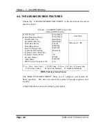
4-4. THE ADVANCED BIOS FEATURES 

 
Choose the

ADVANCED BIOS FEATURES

in the main menu, the screen 

shown as below. 
 

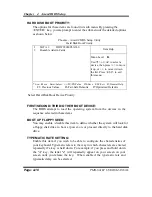
Phoenix - AwardBIOS CMOS Setup Utility 

Advanced BIOS Features 

Item Help 


CPU Feature 


Hard Disk Boot Priority 

First Boot Device 
Second Boot Device 
Third Boot Device 
Boot Other Device 
Boot Up Floppy Seek 
Typematic Rate Setting 


x


Typematic Rate (Chars/Sec) 


x


Typematic Delay (Msec) 

Security Option 
APIC Mode 
MPS Version Control For OS   
 

[Press Enter] 
[Press Enter] 
[Hard Disk] 
[Hard Disk] 
[LS120] 
[Enabled] 
[Enabled] 
[Disabled] 

250 
[Setup] 
[Enabled] 
[1.4] 

Menu Level   


↑↓→←

: Move  Enter: Select  +/-/PU/PD:Value  F10:Save  ESC:Exit  F1:General Help 

   F5: Previous Values    F6: Fail-Safe Defaults   F7:Optimized Defaults 

BIOS Features Setup Screen 

 
The “BIOS FEATURES SETUP” allow you to configure your system for 
basic operation.  The user can select the system’s boot-up sequence and 
security. 
 
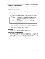
A brief introduction of each setting is given below. 

Содержание PMB-601LF

Страница 1: ...USER S MANUAL PMB 601LF Intel Core 2 Duo ATX Motherboard With VGA Sound 2LAN PMB 601LF M1 ...

Страница 2: ... subject to change without any notice This manual is copyrighted in January 2007 You may not reproduce or transmit in any form or by any means electronic or mechanical including photocopying and recording ACKNOWLEDGEMENTS All trademarks and registered trademarks mentioned herein are the property of their respective owners CE NOTICE This is a class A product In a domestic environment this product m...

Страница 3: ...es uses and can radiate radio frequency energy and if not installed and used in accordance with the instruction manual may cause harmful interference to radio communications Operation of this equipment in a residential area is likely to cause harmful interference in which case the user will be required to correct the interference at his own expense You are cautioned that any change or modification...

Страница 4: ...2 10 Hard Disk Drive LED Connector 2 12 2 11 ATX Power Button 2 12 2 12 External Speaker Connector 2 12 2 13 PLED Connector 2 13 2 14 KeyLock Connector 2 13 2 15 External SMI Connector 2 13 2 16 Clear CMOS Data Selection 2 14 2 17 CPU Fan Connector 2 14 2 18 System Fan Connector 2 15 2 19 Power Fan Connector 2 15 2 20 NB Fan Connector 2 15 2 21 VGA Connector 2 16 2 22 Serial ATA Connector 2 17 2 2...

Страница 5: ...e Standard CMOS Features 4 4 4 4 The Advanced BIOS Features 4 8 4 5 Advanced Chipset Features 4 12 4 6 Integrated Peripherals 4 14 4 7 Power Management Setup 4 19 4 8 PNP PCI Configuration 4 21 4 9 PC Health Status 4 23 4 10 Frequency Control 4 24 4 11 Load Fail Safe Defaults 4 25 4 12 Load Optimized Defaults 4 25 4 13 Password Setting 4 26 4 14 Save Exit Setup 4 27 4 15 Exit Without Saving 4 28 A...

Страница 6: ...s you the information for PMB 601LF It also outlines the System specifications Section includes z About This Manual z System Specifications z Safety Precautions Experienced users can skip to chapter 2 on page 2 1 for a Quick Start CHAPTER 1 ...

Страница 7: ...m The final page of this chapter will indicate how to avoid damaging this board Chapter 2 Hardware Configuration This chapter outlines the component locations and their functions In the end of this chapter you will learn how to set jumper and how to configure this card to meet your own needs Chapter 3 Software Utilities This chapter contains helpful information for proper installations of the VGA ...

Страница 8: ...gulator z CHIPSET Intel Q965 ICH8DO FWH z MEMORY Supports up to 8GB DDR SDRAM Four 240 pin DDR2 DIMM sockets on board z CACHE Built in CPU z REAL TIME CLOCK Build in South Bridge z BIOS Phoenix AwardBIOS for plug play function 8Mb with VGA BIOS Easy update 1MB flash EEPROM Support S IO Setup z KEYBOARD CONNECTOR Mini DIN connector Supports for AT PS2 keyboard z MOUSE CONNECTOR Mini DIN connector S...

Страница 9: ...ives 3 5 and 5 25 360K 720K 1 2M 1 44M 2 88M z USB CONNECTOR Support up to ten USB 2 0 ports 4 ports with LAN1 LAN2 on rear panel 6 ports with external 2 54 connector 2x5 pin headpin z LAN ADAPTER Dual ports Intel 82573V x 2 10 100 1000 BaseT Ethernet LAN1 10 100 1000 BaseT Ethernet LAN2 10 100 1000 BaseT Ethernet Support wake on LAN function z SOUND Realtek ALC262A HD Codec including SPDIF Fully ...

Страница 10: ...RT 5 pin Infrared port support IrDA v1 0 SIR protocol z PARALLEL PORT SPP ECP EPP Function 1 port bi directional parallel port z GREEN FUNCTION Controlled by hardware and software z LED INDICATOR System power Hard Disk access SATA z DMA CONTROLLER 82C37 x 2 z DMA CHANNELS 7 z INTERRUPT CONTROLLERS 82C59 x 2 z INTERRUPT LEVELS 15 z OPERATING TEMPERATURE 0 to 60 C z BOARD DIMENSIONS 305mm x 344mm 12...

Страница 11: ...static electricity on all occasions 2 Prevent electric shock Don t touch any components of this card when the card is power on Always disconnect power when the system is not in use 3 Disconnect power when you change any hardware devices For instance when you connect a jumper or install any cards a surge of power may damage the electronic components or the whole system ...

Страница 12: ...RT CHAPTER 2 Helpful information describes the jumper connector settings and component locations Section includes z Jumper Connector Quick Reference Table z Component Locations z Configuration and Jumper settings z Connector s Pin Assignments ...

Страница 13: ... JP8 14 16 18 20 PLED Connector JP8 2 4 KeyLock Connector JP8 13 15 External SMI Connector JP8 17 19 Clear CMOS Data Selection JP4 CPU Fan Connector CPU_FAN1 System Fan Connector SYS_FAN1 Power Fan Connector PWR_FAN1 NB Fan Connector NB_FAN1 VGA Connector VGA1 Serial ATA Connector SATA1 SATA2 SATA3 SATA4 Floppy Disk Drive Connector FDD1 Printer Connector LPT1 Universal Serial Bus Connector USB1 US...

Страница 14: ...Chapter 2 Hardware Configuration PMB 601LF USER S MANUAL Page 2 3 2 2 COMPONENT LOCATIONS PMB 601LF Connector Jumper and Component locations ...

Страница 15: ...nfiguration by open or close pins The jumper can be combined into sets that called jumper blocks When the jumpers are all in the block you have to put them together to set up the hardware configuration The figure below shows how this looks like JUMPERS AND CAPS If a jumper has three pins for examples labelled PIN1 PIN2 and PIN3 You can connect PIN1 PIN2 to create one setting by shorting You can ei...

Страница 16: ...in Jumper looks like this Jumper Cap looks like this 3 pin Jumper looks like this Jumper Block looks like this JUMPER SETTINGS Looks like this 3 pin Jumper 2 3 pin close enabled Looks like this Jumper Block 1 2 pin close enabled 2 pin Jumper close enabled 1 1 1 2 1 2 1 1 Looks like this ...

Страница 17: ...ENT 1 COM1_DCD 2 COM1_RX 3 COM1_TX 4 COM1_DTR 5 GND 6 COM1_DSR 7 COM1_RTS 8 COM1_CTS 9 COM1_RI COM2 COM2 Connector The COM2 is selectable as RS 232 422 485 The pin assignment is as follows ASSIGNMENT PIN RS 232 RS 422 RS 485 1 COM2_DCD TX TX 2 COM2_RX TX TX 3 COM2_TX RX RX 4 COM2_DTR RX RX 5 GND GND GND 6 COM2_DSR RTS GND 7 COM2_RTS RTS GND 8 COM2_CTS CTS GND 9 COM2_RI CTS GND ...

Страница 18: ...in assignment is as follows PIN ASSIGNMENT 1 COM3_DCD 2 COM3_RX 3 COM3_TX 4 COM3_DTR 5 GND 6 COM3_DSR 7 COM3_RTS 8 COM3_CTS 9 COM3_RI COM4 COM4 Connector COM4 is fixed as RS 232 The pin assignment is as follows PIN ASSIGNMENT 1 COM4_DCD 2 COM4_RX 3 COM4_TX 4 COM4_DTR 5 GND 6 COM4_DSR 7 COM4_RTS 8 COM4_CTS 9 COM4_RI ...

Страница 19: ...iguration Page 2 8 PMB 601LF USER S MANUAL 2 5 COM3 RI VOLTAGE SELECTION JP6 COM3 RI Voltage Selection The selections are as follows SELECTION JUMPER SETTINGS JUMPER ILLUSTRATION 5V 5 6 12V 3 4 RI 1 2 Manufacturing Default RI ...

Страница 20: ...iguration PMB 601LF USER S MANUAL Page 2 9 2 6 COM4 RI VOLTAGE SELECTION JP7 COM4 RI Voltage Selection The selections are as follows SELECTION JUMPER SETTINGS JUMPER ILLUSTRATION 5V 5 6 12V 3 4 RI 1 2 Manufacturing Default RI ...

Страница 21: ...485 COM2 SELECTION JP5 RS 232 422 485 COM2 Selection This connector is used to set the COM2 function The jumper settings are as follows COM 2 Function Jumper Settings pin closed Jumper Illustrations RS 232 All Open RS 422 1 2 3 4 9 10 RS 485 1 2 5 6 7 8 Manufacturing default RS 232 ...

Страница 22: ...SE CONNECTOR KB_MS1 Keyboard and PS 2 Mouse Connector The pin assignments are as follows PIN ASSIGNMENT 1 KBDATA 2 NC 3 GND 4 VCC5 5 KBCLK 6 NC 7 MSDATA 8 NC 9 GND 10 VCC5 11 MSCLK 12 NC 2 9 RESET CONNECTOR JP8 5 7 Reset Connector The pin assignment is as follows PIN ASSIGNMENT 5 GND 7 RST_BTN ...

Страница 23: ...gnment is as follows PIN ASSIGNMENT 1 HD_LED 3 HD_LED 2 11 ATX POWER BUTTON JP8 6 8 ATX Power Button The pin assignment is as follows PIN ASSIGNMENT 6 PWRBTNSW 8 GND 2 12 EXTERNAL SPEAKER CONNECTOR JP8 14 16 18 20 External Speaker Connector The pin assignment is as follows PIN ASSIGNMENT 14 SPK_VCC 16 SPEAKER SIGNAL 18 SPEAKER SIGNAL 20 SPEAKER SIGNAL ...

Страница 24: ... The pin assignment is as follows PIN ASSIGNMENT 2 PW_LED 4 PW_LED 2 14 KEYLOCK CONNECTOR JP8 13 15 Keylock Connector The pin assignment is as follows PIN ASSIGNMENT 13 KEYLOCK 15 GND 2 15 EXTERNAL SMI CONNECTOR JP8 17 19 External SMI Connector The pin assignment is as follows PIN ASSIGNMENT 17 SLP_BTN 19 GND ...

Страница 25: ...ILLUSTRATION Normal 1 2 Clear CMOS 2 3 Manufacturing Default Normal Note To clear CMOS data user must power off the computer and set the jumper to Clear CMOS as illustrated above After five to six seconds set the jumper back to Normal and power on the computer 2 17 CPU FAN CONNECTOR CPU_FAN1 CPU Fan connector The pin assignment is as follows PIN ASSIGNMENT 1 GND 2 VCC12 3 LPC1_FANIO1 4 LPC1_FANPWM...

Страница 26: ...The pin assignment is as follows PIN ASSIGNMENT 1 GND 2 VCC12 3 LPC1_FANIO2 2 19 POWER FAN CONNECTOR PWR_FAN1 Power Fan connector The pin assignment is as follows PIN ASSIGNMENT 1 GND 2 VCC12 3 LPC1_FANIO3 2 20 NB FAN CONNECTOR NB_FAN1 North Bridge Fan connector The pin assignment is as follows PIN ASSIGNMENT 1 GND 2 VCC12 ...

Страница 27: ...Hardware Configuration Page 2 16 PMB 601LF USER S MANUAL 2 21 VGA CONNECTOR VGA1 VGA Connector PIN ASSIGNMENT 1 RED 2 GREEN 3 BLUE 4 NC 5 GND 6 GND 7 GND 8 GND 9 VCC 10 GND 11 NC 12 DATA 13 HSYNC 14 VSYNC 15 CLK ...

Страница 28: ...R SATA1 SATA4 The PMB 601LF possesses four Serial ATA Connector SATA1 SATA4 The pin assignments are as follows SATA1 PIN ASSIGNMENT 1 GND 2 SATA_TXPC4 3 SATA_TXNC4 4 GND 5 SATA_RXNC4 6 SATA_RXPC4 7 GND SATA2 PIN ASSIGNMENT 1 GND 2 SATA_TXPC5 3 SATA_TXNC5 4 GND 5 SATA_RXNC5 6 SATA_RXPC5 7 GND ...

Страница 29: ...TA_TXPC0 3 SATA_TXNC0 4 GND 5 SATA_RXNC0 6 SATA_RXPC0 7 GND 8 GND 9 SATA_TXPC1 10 SATA_TXNC1 11 GND 12 SATA_RXNC1 13 SATA_RXPC1 14 GND SATA4 PIN ASSIGNMENT 1 GND 2 SATA_TXPC2 3 SATA_TXNC2 4 GND 5 SATA_RXNC2 6 SATA_RXPC2 7 GND 8 GND 9 SATA_TXPC3 10 SATA TXNC3 11 GND 12 SATA_RXNC3 13 SATA_RXPC3 14 GND ...

Страница 30: ...in flat cable to attach the FDD on the board and the other side is attaches two FDDs The pin assignments are as follows PIN ASSIGNMENT PIN ASSIGNMENT 1 GND 2 F_DENSEL 3 GND 4 NC 5 GND 6 NC 7 GND 8 F_INDEX 9 GND 10 F_MTRA 11 GND 12 F_DRVB 13 GND 14 F_DRVA 15 GND 16 F_MTRB 17 GND 18 F_DIR 19 GND 20 F_STEP 21 GND 22 F_WDATA 23 GND 24 F_WGATE 25 GND 26 F_TRK0 27 GND 28 F_WPT 29 GND 30 F_RDATA 31 GND 3...

Страница 31: ...inter to the card you need a cable to connect both DB25 connector and parallel port The pin assignments are as follows PIN ASSIGNMENT PIN ASSIGNMENT 1 STB 14 AFD 2 PDR0 15 ERR 3 PDR1 16 INIT 4 PDR2 17 SLIN 5 PDR3 18 GND 6 PDR4 19 GND 7 PDR5 20 GND 8 PDR6 21 GND 9 PDR7 22 GND 10 ACK 23 GND 11 BUSY 24 GND 12 PE 25 GND 13 SLCT 26 NC ...

Страница 32: ...al Serial Bus Connector The pin assignments are as follows PIN ASSIGNMENT 1 USB4_VCC5 2 USBN8 3 USBP8 4 GND 5 NC 6 USB4_VCC5 7 USBN9 8 USBP9 9 GND 10 NC USB2 Universal Serial Bus Connector The pin assignments are as follows PIN ASSIGNMENT 1 USB3_VCC5 2 USBN6 3 USBP6 4 GND 5 NC 6 USB3_VCC5 7 USBN7 8 USBP7 9 GND 10 NC ...

Страница 33: ...l Serial Bus Connector The pin assignments are as follows PIN ASSIGNMENT 1 USB2_VCC5 2 USBN4 3 USBP4 4 GND 5 NC 6 USB2_VCC5 7 USBN5 8 USBP5 9 GND 10 NC 2 26 IRDA CONNECTOR JP1 IrDA Infrared Connector The pin assignments are as follows PIN ASSIGNMENT 1 VCC5 2 NC 3 IRRX 4 GND 5 IRTX ...

Страница 34: ...CTOR USB_RJG2 USB LAN Connector The pin assignments are as follows LAN PIN ASSIGNMENT 1 LAN1_TXDP 2 LAN1_TXDN 3 LAN1_RXDP 4 LAN1_RXDN 11 LAN1_LILED 12 LAN1_ACTLED 13 LAN1_SPD100 14 LAN1_LEDVCC USB PIN ASSIGNMENT A1 USB0_VCC5 A2 USBN0 A3 USBP0 A4 GND B1 USB0_VCC5 B2 USBN1 B3 USBP1 B4 GND ...

Страница 35: ...nts are as follows LAN PIN ASSIGNMENT 1 LAN2_1MDI_P0 2 LAN2_1MDI_N0 3 LAN2_1MDI_P1 4 LAN2_1MDI_N1 5 LAN2_1MDI_P2 6 LAN2_1MDI_N2 7 LAN2_1MDI_P3 8 LAN2_1MDI_N3 11 LAN2_LILED 12 LAN2_ACTLED 13 LAN2_SPD100 14 LAN2_SPD1000 USB PIN ASSIGNMENT A1 USB1_VCC5 A2 USBN2 A3 USBP2 A4 GND B1 USB1_VCC5 B2 USBN3 B3 USBP3 B4 GND ...

Страница 36: ... pin assignments are as follows PIN ASSIGNMENT 1 GND 2 GND 3 12V 4 12V ATX_PW2 ATX Power Connector The pin assignments are as follows PIN ASSIGNMENT PIN ASSIGNMENT 1 3 3V 13 3 3V 2 3 3V 14 12V 3 GND 15 GND 4 5V 16 PSON 5 GND 17 GND 6 5V 18 GND 7 GND 19 GND 8 POK 20 5V 9 5VSB 21 5V 10 12V 22 5V 11 12V 23 5V 12 3 3V 24 GND ...

Страница 37: ...Connector including Line In Line Out Mic Also can support only MIC connector The pin assignments are as follows Line In PIN ASSIGNMENT 32 HD_LINE L 33 GND 34 GND 35 HD_LINE R Line Out PIN ASSIGNMENT 22 HD_OUT L 23 NC 24 NC 25 HD_OUT R Mic In PIN ASSIGNMENT 1 GND 2 HD_MIC1 3 HD_MIC_GND 4 NC 5 HD_MIC_VCC ...

Страница 38: ...nts are as follows PIN ASSIGNMENT 1 CD L 2 CD REF 3 CD REF 4 CD R 2 31 MEMORY INSTALLATION PMB 601LF CPU Card can support up to 4GB in four DIMM sockets DRAM BANK CONFIGURATION DIMM 1 DIMM 2 DIMM3 DIMM4 TOTAL MEMORY 128MB 128MB 128MB 128MB 512MB 256MB 256MB 256MB 256MB 1GB 512MB 512MB 512MB 512MB 2GB 1GB 1GB 1GB 1GB 4GB 2GB 2GB 2GB 2GB 8GB ...

Страница 39: ... BIOS update It also describes on how to configuration the watchdog timer Section includes z Introduction z VGA Driver Utility z Flash BIOS Update z LAN Driver Utility z Sound Driver Utility z Intel Chipset Software Installation Utility z USB2 0 Chipset Software Installation Utility z Watchdog Timer Configuration CHAPTER 3 ...

Страница 40: ... VGA Intel Q965 For VGA driver installation D Driver FLASH For BIOS update utility D Driver LAN For LAN Driver installation D Driver Sound Realtek ALC262A Audio HD For Sound driver installation D Driver UTILITY Intel Chipset Software Installation Utility For Win 2000 XP 2003 D Driver RAID Intel ICH8 R RAID Software Installation Utility For Win 2000 XP 2003 D Driver USB 2 0 USB 2 0 Software Install...

Страница 41: ...f VGA Driver To install the VGA Driver simply follow the following steps 1 Place insert the Utility Disk into Floppy Disk Drive A B or CD ROM drive 2 Under Windows 2000 XP 2003 system go to the directory where VGA driver is located 3 Click Setup exe file for VGA driver installation 4 Follow the instructions on the screen to complete the installation 5 Once installation is completed shut down the s...

Страница 42: ...from the CD ROM Disk into your system 2 Insert the new BIOS file you have obtained from Protech 3 Type the pathname to Awdflash exe and execute the BIOS update with file B601xxxx bin C UTIL AWDFLASH AWARDFLASH B601xxxx bin 4 The screen will display the table below AwardBIOS Flash Utility V8 69 C Phoenix Technologies Ltd All Rights Reserved For Broadwater 6A79LP69C 00 DATE 01 16 2007 Flash Type SST...

Страница 43: ...adwater 6A79LP69C 00 DATE 01 16 2007 Flash Type SST 49LF008A 3 3V File Name to Program B601xxxx bin Message Press Y to Program or N to Exit Select Y and the BIOS will be renewed When you are refreshing your BIOS do not turn off or reset the system or you will damage the BIOS After you have completed all the programming you will see the line Reset System or power off to accomplish update process Pl...

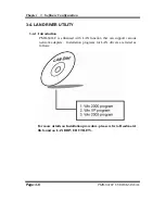
Страница 44: ...RIVER UTILITY 3 4 1 Introduction PMB 601LF is enhanced with LAN function that can support various network adapters Installation programs for LAN drivers are listed as follows For more details on Installation procedure please refer to Readme txt file found on LAN DRIVER UTILITY ...

Страница 45: ... Below you will find the content of the Sound driver 3 5 2 Installation Procedure for Windows 2000 XP 2003 1 From the task bar click on Start and then Run 2 In the Run dialog box type D Sound path setup where D Sound pathname refers to the full path to the source files 3 Click on the OK button or press the ENTER key 4 Click on the Next and OK prompts as they appear 5 Reboot the system to complete ...

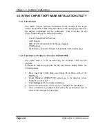
Страница 46: ...Support Identification of Intel Chipset Components in Device Manager 3 6 2 Installation of Utility for Windows 2000 XP 2003 The Utility Pack is to be installed only for Windows 2000 and XP program It should be installed right after the OS installation kindly follow the following steps 1 Place insert the Utility Disk into Floppy Disk Drive A B or CD ROM drive 2 Under Windows 2000 XP 2003 system go ...

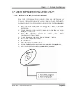
Страница 47: ... kindly follow the following steps 1 Place insert the Utility Disk into Floppy Disk Drive A B or CD ROM drive 2 Under Windows 2000 and XP system go to the directory where Utility Disc is located 3 Start the System wizard in control panel Click Start Settings Control Panel 4 Select Hardware and click Device Manager button 5 Double Click USB Root Hub 6 Select Driver 7 Click Install to install the dr...

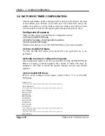
Страница 48: ...ation registers 3 Exit the MB PnP Mode Undesired result may occur if the MB PnP Mode is not exited normally 1 Enter the MB PnP Mode To enter the MB PnP Mode four special I O write operations are to be performed 2 Modify the data of configuration registers All configuration registers can be accessed after entering the MB PnP Mode Before accessing a selected register the content of index 07h must be...

Страница 49: ...inute resolution MOVDX 2Eh MOVAL 72h OUTDX AL MOVDX 2Fh MOVAL 0C0h OUTDX AL Write non zero value into index 73h for Enable WDT and Start count down MOVDX 2Eh MOVAL 73h OUTDX AL MOVDX 2Fh MOVAL 02h OUTDX AL Write zero value into register AL for Disable WDT MOVDX 2Eh MOVAL 73h OUTDX AL MOVDX 2Fh MOVAL 00h OUTDX AL Exit PnP Mode MOVDX 2Eh MOVAL 02h OUTDX AL MOVDX 2Fh MOVAL 02h OUTDX AL ...

Страница 50: ... The Standard CMOS Features z The Advanced BIOS Features z The Advanced Chipset Features z Integrated Peripherals z Power Management Setup z PNP PCI Configuration z PC Health Status z Frequency Control z Load Fail Safe Defaults z Load Optimized Defaults z Password Setting z Save and Exit Setup z Exit Without Saving CHAPTER 4 ...

Страница 51: ...Your application programs such as word processing spreadsheets and games rely on an operating system such as DOS or OS 2 to manage such things as keyboard monitor disk drives and memory The operating system relies on the BIOS Basic Input and Output system a program stored on a ROM Read only Memory chip to initialize and configure your computer s hardware As the interface between the hardware and t...

Страница 52: ... the Award SETUP program will appear on the screen Phoenix AwardBIOS CMOS Setup Utility Standard CMOS Features Advanced BIOS Features Advanced Chipset Features Integrated Peripherals Power Management Setup PnP PCI Configurations PC Health Status Frequency Control Load Fail Safe Defaults Load Optimized Defaults Set Supervisor Password Set User Password Save Exit Setup Exit Without Saving Esc Quit S...

Страница 53: ...380 None None None None None 1 44M 3 5 in EGA VGA All But Keyboard 640K 514048K 515072K Menu Level Change the day month year and century Move Enter Select PU PD Value F10 Save ESC Exit F1 General Help F5 Previous Values F6 Fail Safe Defaults F7 Optimized Defaults CMOS Setup screen In the above Setup Menu use the arrow keys to highlight the item and then use the PgUp or PgDn keys to select the valu...

Страница 54: ... drive specifications Type The BIOS contains a table of pre defined drive types Each defined drive type has a specified number of cylinders number of heads write precompensation factor landing zone and number of sectors Drives whose specifications do not accommodate any predefine type are classified as type USER Size Disk drive capacity approximate Note that this size is usually greater than the s...

Страница 55: ... to select the type in Setup Available Options are as follows EGA VGA Enhanced Graphics Adapter Video Graphics Array For EGA VGA SEGA SVGA or PGA monitor adapters CGA 40 Color Graphics Adapter power up in 40 column mode CGA 80 Color Graphics Adapter power up in 80 column mode MONO Monochrome adapter includes high resolution monochrome adapters HALT ON This category allows user to choose whether th...

Страница 56: ... 56 19 1024 7 512 1023 17 59 20 733 5 300 732 17 30 21 733 7 300 732 17 42 22 733 5 300 733 17 30 23 306 4 0000 336 17 10 24 977 5 65535 976 17 40 25 1024 9 65535 1023 17 76 26 1224 7 65535 1223 17 71 27 1224 11 65535 1223 17 111 28 1224 15 65535 1223 17 152 29 1024 8 65535 1023 17 68 30 1024 11 65535 1023 17 93 31 918 11 65535 1023 17 83 32 925 9 65535 926 17 69 33 1024 10 65535 1023 17 85 34 102...

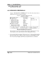
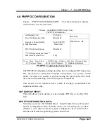
Страница 57: ...ic Rate Setting x Typematic Rate Chars Sec x Typematic Delay Msec Security Option APIC Mode MPS Version Control For OS Press Enter Press Enter Hard Disk Hard Disk LS120 Enabled Enabled Disabled 6 250 Setup Enabled 1 4 Menu Level Move Enter Select PU PD Value F10 Save ESC Exit F1 General Help F5 Previous Values F6 Fail Safe Defaults F7 Optimized Defaults BIOS Features Setup Screen The BIOS FEATURES...

Страница 58: ...y Disabled Enabled Enabled Menu Level Move Enter Select PU PD Value F10 Save ESC Exit F1 General Help F5 Previous Values F6 Fail Safe Defaults F7 Optimized Defaults Descriptions on each item above are as follows 1 LIMIT CPUID MAXVAL The CPUID instruction of some CPUs will return a value greater than 3 If you are using Windows operating system Please disable this feature 2 EXECUTE DISABLE BIT To se...

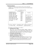
Страница 59: ...ptimized Defaults Select Hard Disk Boot Device Priority FIRST SECOND THIRD OTHER BOOT DEVICE The BIOS attempt to load the operating system from the devices in the sequence selected in these items BOOT UP FLOPPY SEEK You may enable disable this item to define whether the system will look for a floppy disk drive to boot at power on or proceed directly to the hard disk drive TYPEMATIC RATE SETTING En...

Страница 60: ... system will boot but access to Setup will be denied if the correct password is not entered at the prompt To disable security select PASSWORD SETTING at Main Menu and then you will be asked to enter password Do not type anything and just press Enter it will disable security Once the security is disabled the system will boot and you can enter Setup freely APIC MODE To Enable Advanced Programmable I...

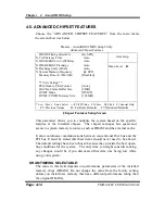
Страница 61: ...ed Defaults Chipset Features Setup Screen This parameter allows you to configure the system based on the specific features of the installed chipset The chipset manages bus speed and access to system memory resources such as DRAM and the external cache It also coordinates communications between conventional ISA bus and the PCI bus It must be stated that these items should never need to be altered T...

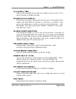
Страница 62: ...ain data Fast gives faster performance and Slow gives more stable performance This field applies only when synchronous DRAM is installed in the system The choices are 2 3 PRECHARGE DEALY tRAS Precharge Delay This setting controls the precharge delay which determines the timing delay for DRAM precharge SYSTEM MEMORY FREQUENCY Allow to choose different frequency of memory module MEMORY HOLE AT 15 16...

Страница 63: ...ard Lan1 Controller Onboard Lan2 Controller Press Enter Press Enter 3E8 IRQ10 2E8 IRQ11 Press Enter Enabled Enabled Menu Level Move Enter Select PU PD Value F10 Save ESC Exit F1 General Help F5 Previous Values F6 Fail Safe Defaults F7 Optimized Defaults Integrated Peripherals Setup Screen By moving the cursor to the desired selection and by pressing the F1 key the all options for the desired selec...

Страница 64: ...mber of block read writes per sector the drive can support Move Enter Select PU PD Value F10 Save ESC Exit F1 General Help F5 Previous Values F6 Fail Safe Defaults F7 Optimized Defaults Descriptions on each item above are as follows 1 IDE HDD BLOCK MODE Block mode is also called block transfer multiple commands or multiple sector read write If your IDE hard drive supports block mode most new drive...

Страница 65: ...he sub menu of the detailed options as shown below Phoenix Award CMOS Setup Utility SuperIO Device Item Help Onboard FDC Controller Onboard Serial Port 1 Onboard Serial Port 2 UART Mode Select X UR2 Duplex Mode Onboard Parallel Port Parallel Port Mode X ECP Mode Use DMA PWRON After PWR Fail Enabled 3F8 IRQ4 2F8 IRQ3 Normal Half 378 IRQ7 SPP 3 Off Menu Level Move Enter Select PU PD Value F10 Save E...

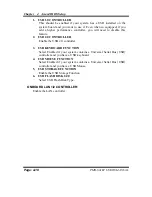
Страница 66: ...ant to power on the system after power failure The choice Off On Former Sts ONBOARD SERIAL PORT 3 4 SERIAL PORT 3 4 USE IRQ Select an address and corresponding interrupt for third and forth serial port USB DEVICE SETTING The options for these items are found in its sub menu By pressing the ENTER key you are prompt to enter the sub menu of the detailed options as shown below Phoenix Award CMOS Setu...

Страница 67: ... this feature 2 USB 2 0 CONTROLLER Enable the USB 2 0 controller 3 USB KEYBOARD FUNCTION Select Enabled if your system contains a Universal Serial Bus USB controller and you have a USB keyboard 4 USB MOUSE FUNCTION Select Enabled if your system contains a Universal Serial Bus USB controller and you have a USB Mouse 5 USB STORAGE FUNCTION Enable the USB Storage Function 6 USB FLASH DISK 2 00 Select...

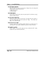
Страница 68: ...d Mode Soft Off by PWR BTTN Wake Up by PCI card Resume by Alarm X Date of Month Alarm X Time hh mm ss Alarm Menu Level Move Enter Select PU PD Value F10 Save ESC Exit F1 General Help F5 Previous Values F6 Fail Safe Defaults F7 Optimized Defaults Power Management Setup Screen The Power Management Setup allows the user to configure the system to the most effectively save energy while operating in a ...

Страница 69: ...evices except the CPU will be shut off SOFT OFF BY PWR BTTN Pressing the power button for more than 4 seconds forces the system to enter the Soft Off state when the system has hung The choices are Delay 4 Sec and Instant Off WAKE UP BY PCI CARD An input signal on the serial Ring Indicator RI line in other words an incoming call on the modem awakens the system from the soft off state RESUME BY ALAR...

Страница 70: ...aults PNP PCI Configuration Setup Screen The PNP PCI Configuration Setup describes how to configure PCI bus system PCI also known as Personal Computer Interconnect is a system which allows I O devices to operate at speeds nearing the speed of the CPU itself uses when communicating with its own special components This section covers technical items which is strongly recommended for experienced user...

Страница 71: ...ssigned to IRQ 7 assigned to IRQ 9 assigned to IRQ 10 assigned to IRQ 11 assigned to IRQ 12 assigned to IRQ 14 assigned to IRQ 15 assigned to PCI Device PCI Device PCI Device PCI Device PCI Device PCI Device PCI Device PCI Device PCI Device PCI Device Menu Level Legacy ISA for devices compliant with the original PC AT bus specification PCI ISA PnP for devices compliant with the Plug and Play stand...

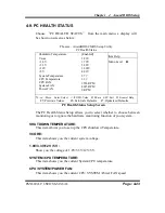
Страница 72: ...lect PU PD Value F10 Save ESC Exit F1 General Help F5 Previous Values F6 Fail Safe Defaults F7 Optimized Defaults PC Health Status Setup Screen The PC Health Status Setup allows you to select whether to choose between monitoring or to ignore the hardware monitoring function of your system SHUTDOWN TEMPERATURE This item allows you to set up the CPU shutdown Temperature VCORE This item shows you the...

Страница 73: ...Control Auto Detect PCI Clk Spread Spectrum Enabled Enabled Item Help Menu Level Move Enter Select PU PD Value F10 Save ESC Exit F1 General Help F5 Previous Values F6 Fail Safe Defaults F7 Optimized Defaults Frequency Voltage Control Setup Screen AUTO DETECT DIMM PCI CLK This item allows you to enable or disable auto detect DIMM PCI Clock SPREAD SPECTRUM This item allows you to enable or disable t...

Страница 74: ...faults Y N N To use the BIOS default values change the prompt to Y and press the Enter key CMOS is loaded automatically when you power up the system 4 12 LOAD OPTIMIZED DEFAULTS When you press Enter on this category you get a confirmation dialog box with a message similar to the following Load Optimized Defaults Y N N Pressing Y loads the default values that are factory setting for optimal perform...

Страница 75: ... in length and press Enter The password typed now will clear any previously entered password from CMOS memory You will be asked to confirm the password Type the password again and press the Enter key You may also press Esc to abort the selection and not enter a password User should bear in mind that when a password is set you will be asked to enter the password everything you enter CMOS setup Menu...

Страница 76: ...d BIOS Features Advanced Chipset Features Integrated Peripherals Power Management PnP PCI Configura PC Health Status Load Fail Safe Defaults Load Optimized Defaults Set Supervisor Password word etup Saving Esc Quit Select Item F10 Save Exit Setup Save Data to CMOS When you confirm that you wish to save the settings your system will be automatically restarted and the changes you have made will be i...

Страница 77: ...CMOS will be retained The screen will be shown as below Phoenix AwardBIOS CMOS Setup Utility Standard CMOS Features Advanced BIOS Features Advanced Chipset Features Integrated Peripherals Power Management PnP PCI Configura PC Health Status Load Fail Safe Defaults Load Optimized Defaults Set Supervisor Password word etup Saving Esc Quit Select Item F10 Save Exit Setup Abandon all Datas Quit Without...

Страница 78: ...Page A 1 EXPANSION BUS This appendix indicates the pin assignments Section includes z PCI BUS Pin Assignment APPENDIX A ...

Страница 79: ... GND A38 STOP B9 REQ3 A9 CLKC B39 LOCK A39 3 3V B10 REQ1 A10 5V I O B40 PERR A40 SDONE B11 GNT3 A11 CLKD B41 3 3V A41 SB0 B12 GND A12 GND B42 SERR A42 GND B13 GND A13 GND B43 3 3V A43 PAR B14 CLKA A14 GNT1 B44 C BE1 A44 AD15 B15 GND A15 RST B45 AD14 A45 3 3V B16 CLKB A16 5V I O B46 GND A46 AD13 B17 GND A17 GNT0 B47 AD12 A47 AD11 B18 REQ0 A18 GND B48 AD10 A48 GND B19 5V I O A19 REQ2 B49 GND A49 AD0...

Страница 80: ...Page B 1 TECHNICAL SUMMARY This section introduce you the maps concisely Section includes z Block Diagram z Interrupt Map z RTC CMOS RAM Map z Timer DMA Channels Map z I O Memory Map APPENDIX B ...

Страница 81: ...Appendix B Technical Summary Page B 2 PMB 601LF USER S MANUAL BLOCK DIAGRAM ...

Страница 82: ...NUAL Page B 3 INTERRUPT MAP IRQ ASSIGNMENT 0 System TIMER 1 Keyboard 2 Cascade 3 Serial port 2 4 Serial port 1 5 Available 6 Floppy 7 Parallel port 1 8 RTC clock 9 Available 10 Available 11 Available 12 PS 2 Mouse 13 Math coprocessor 14 IDE1 15 IDE2 ...

Страница 83: ...0C Status register C 0D Status register D 0E Diagnostic status byte 0F Shutdown byte 10 Floppy Disk drive type byte 11 Reserve 12 Hard Disk type byte 13 Reserve 14 Equipment byte 15 Base memory low byte 16 Base memory high byte 17 Extension memory low byte 18 Extension memory high byte 30 Reserved for extension memory low byte 31 Reserved for extension memory high byte 32 Date Century byte 33 Info...

Страница 84: ...MER DMA CHANNELS MAP Timer Channel Map Timer Channel Assignment 0 System timer interrupt 1 DRAM Refresh request 2 Speaker tone generator DMA Channel Map DMA Channel Assignment 0 Available 1 Available 2 Floppy 3 Available 4 Cascade 5 Available 6 Available 7 Available ...

Страница 85: ... MAP ASSIGNMENT 000 01F DMA controller Master 020 021 Interrupt controller Master 022 023 Chipset controller registers I O ports 040 05F Timer control regsiters 060 06F Keyboard interface controller 8042 070 07F RTC ports CMOS I O ports 080 09F DMA register 0A0 0BF Interrupt controller Slave 0C0 0DF DMA controller Slave 0F0 0FF Math coprocessor 1F0 1F8 Hard Disk controller 278 27F Parallel port 2 ...

Отзывы: