


Design Guide
18 of 48
V 1.0
2018-06-06
XDPL8218 design guide
For high power factor flyback converter with constant voltage output
DC link filter and secondary main output capacitance
10
DC link filter and secondary main output capacitance
C
DC,filter
denotes the DC link filter capacitor placed after the bridge rectifier. A higher C
DC,filter
value gives lower EMI
but worse power quality, and vice versa.
Table 4
Recommended initial C
DC,filter
value
V
AC,min
(V)
Steady-state full-load output power P
out,full
(W)
Recommended initial C
DC,filter
(
𝝁
F)
90 ~ 107
Less than 26
0.1
26 ~ 35
0.15
36 ~ 45
0.22
Greater than 45
Greater than 0.22
Greater than or
equal to 108
Less than 31
0.1
31 ~ 40
0.15
41 ~ 55
0.22
Greater than 55
Greater than 0.22
Referring to
, initial C
DC,filter
= 0.22
𝝁
F is selected in this design example. To improve the estimated input
voltage V
in
accuracy during pre-start-up check, it is also recommended to deploy DC link resistor R
DC,filter
= 30
MΩ in parallel with C
DC,filter
, as shown in
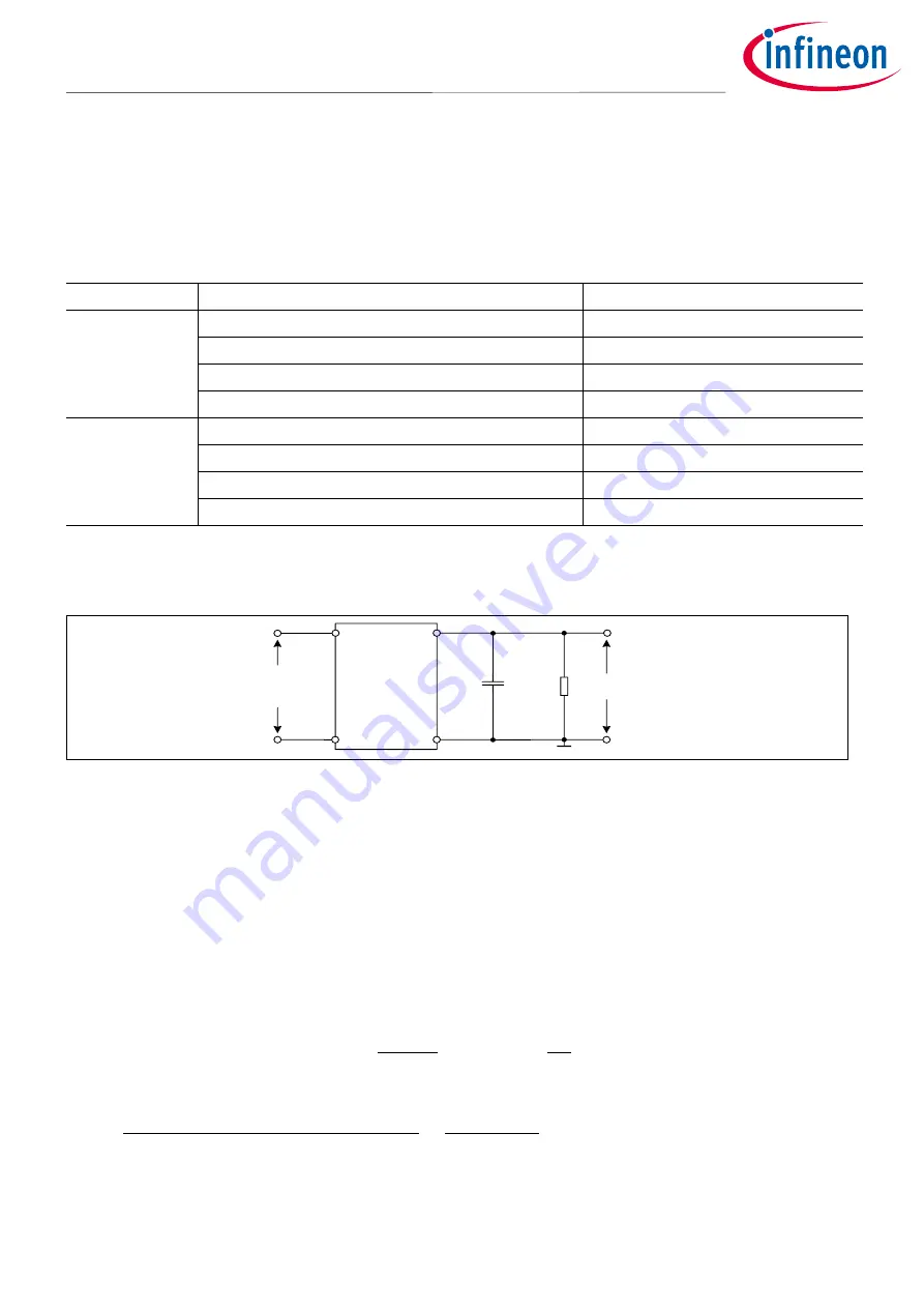
AC
Input
Line Filter
and
Bridge
Rectifier
V
DC,filter
+
-
~
~
C
DC,filter
R
DC,filter
Figure 13
C
DC,filter
and R
DC,filter
across the DC link bus voltage
To compensate for the input current displacement caused by the C
DC,filter
, the XDPL8218 enhanced Power Factor
Correction (PFC) feature can be enabled by configuration of the compensation gain parameter named C
EMI
. As a
start, it can be configured as per the C
DC,filter
value. Hence, the initial C
EMI
= 0.22
𝝁
F parameter setting is selected
in this design example. Upon successful powering-up of the sytem, refer to
Section 18.3
guide.
V
ripple,out(pk-pk),max
denotes the maximum allowable secondary main output voltage peak-to-peak ripple level.
Assuming the flyback output in this design example is connected to a second-stage CC buck regulator, which
has a maximum LED voltage load V
LED,max
of 48 V and maximum allowable duty cycle D
buck,max
of 95 percent,
V
ripple,out(pk-pk),max
can be defined and calculated as:
𝑉
𝑟𝑖𝑝𝑝𝑙𝑒,𝑜𝑢𝑡(𝑝𝑘−𝑝𝑘),𝑚𝑎𝑥
= 2 ∙ (𝑉
𝑜𝑢𝑡,𝑠𝑒𝑡𝑝𝑜𝑖𝑛𝑡
−
𝑉
𝐿𝐸𝐷,𝑚𝑎𝑥
𝐷
𝑏𝑢𝑐𝑘,𝑚𝑎𝑥
) = 2 ∙ (54 −
48
0.95
) = 6.95 𝑉
(28)
The secondary main output capacitor C
out
value can then be defined and calculated as:
𝐶
𝑜𝑢𝑡
≥
𝑃
𝑜𝑢𝑡,𝑓𝑢𝑙𝑙
2𝜋 ∙ 𝐹
𝑙𝑖𝑛𝑒,𝑚𝑖𝑛
∙ 𝑉
𝑟𝑖𝑝𝑝𝑙𝑒,𝑜𝑢𝑡(𝑝𝑘−𝑝𝑘),𝑚𝑎𝑥
∙ 𝑉
𝑜𝑢𝑡,𝑠𝑒𝑡𝑝𝑜𝑖𝑛𝑡
=
43.2
2𝜋 ∙ 47 ∙ 6.95 ∙ 54
= 390 µ𝐹
(29)
Considering the tolerance of the electrolytic capacitor value, C
out
= 470
𝝁
F is selected in this design example.
For lower EMI, low-ESR ceramic capacitors C
out,lowESR1
= 1
𝝁
F and C
out,lowESR2
= 0.1
𝝁
F are also added in parallel
with C
out
.


